ZL40218 Data Sheet
6
Microsemi Corporation
3.0 Functional Description
The ZL40218 is an LVDS clock fanout buffer with eight identical output clock drivers capable of operating at
frequencies up to 750MHz.
Inputs to the ZL40218 are externally terminated to allow use of precision termination components and to allow full
flexibility
of input termination. The ZL40218 can accept DC or AC coupled LVPECL, LVDS, CML or HCSL input
signals; single ended input signals can also be accepted. A pin compatible device with internal termination is also
available.
The ZL40218 is designed to fan out
low-jitter reference clocks for wired or optical communications applications
while adding minimal jitter to the clock signal. An internal linear power supply regulator and bulk capacitors
minimize additive jitter due to power supply noise. The device operates from 2.5V+/-5% or 3.3V+/-5% supply. Its
operation is guaranteed over the industrial temperature range -40°C to +85°C.
The device block diagram is shown in Figure 1; its operation is described in the following sections.
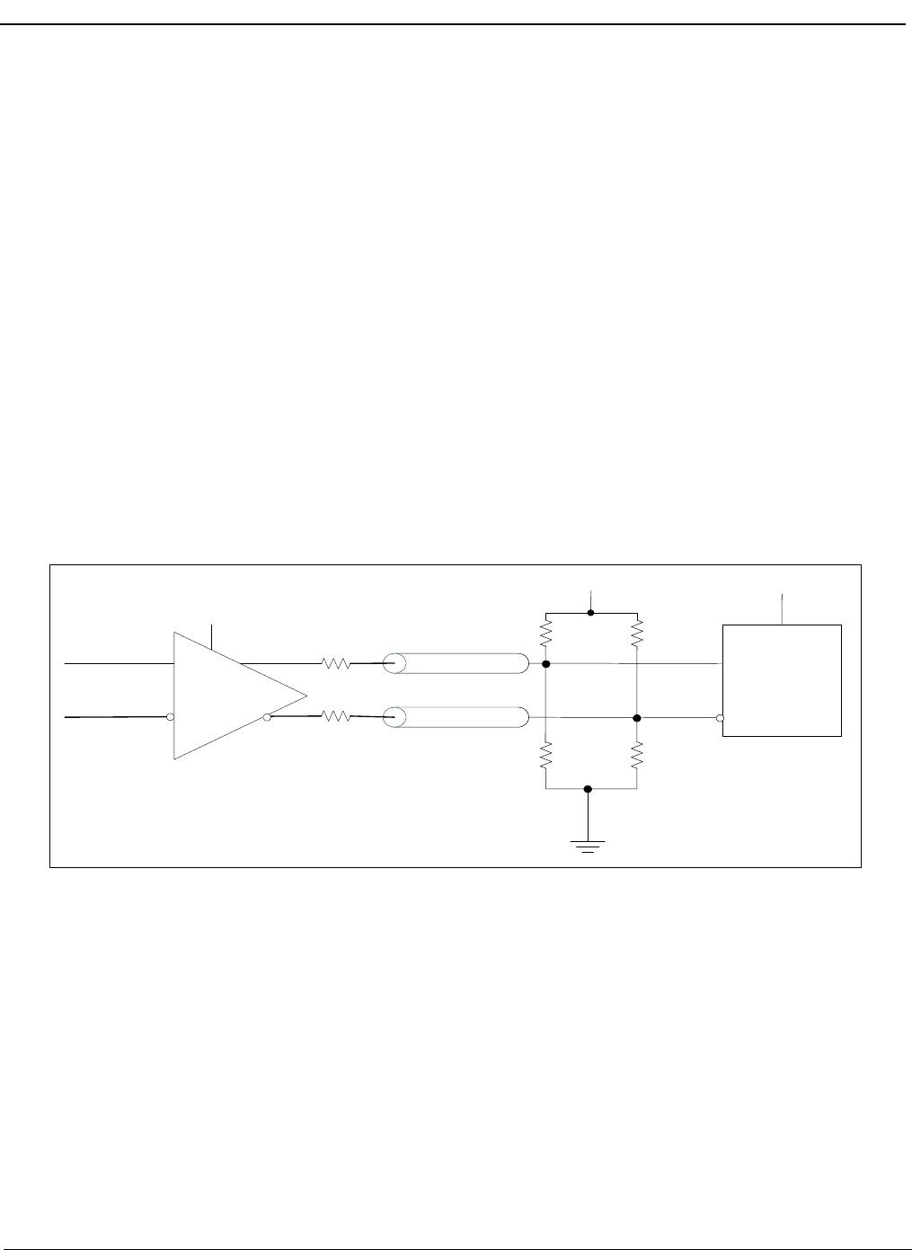
3.1 Clock Inputs
The ZL40218 is adaptable to support different types of differential and singled-ened input signals depending on the
passive components used in the input termination. The application diagrams in the following figures allow the
ZL40218 to accept LVPECL, LVDS, CML, HCSL and single-ended inputs.
VDD_driver
R2 R2
R1 R1
VDD_driver
VDD
VDD_driver=3.3V: R1=127 ohm, R2=82 ohm
VDD_driver=2.5V: R1=250 ohm, R2=62.5 ohm
ZL40218
clk_p
clk_n
Z
o
= 50 Ohms
Z
o
= 50 Ohms
LVPECL
Driver
22 Ohms
22 Ohms
Figure 3 - LVPECL Input DC Coupled Thevenin Equivalent