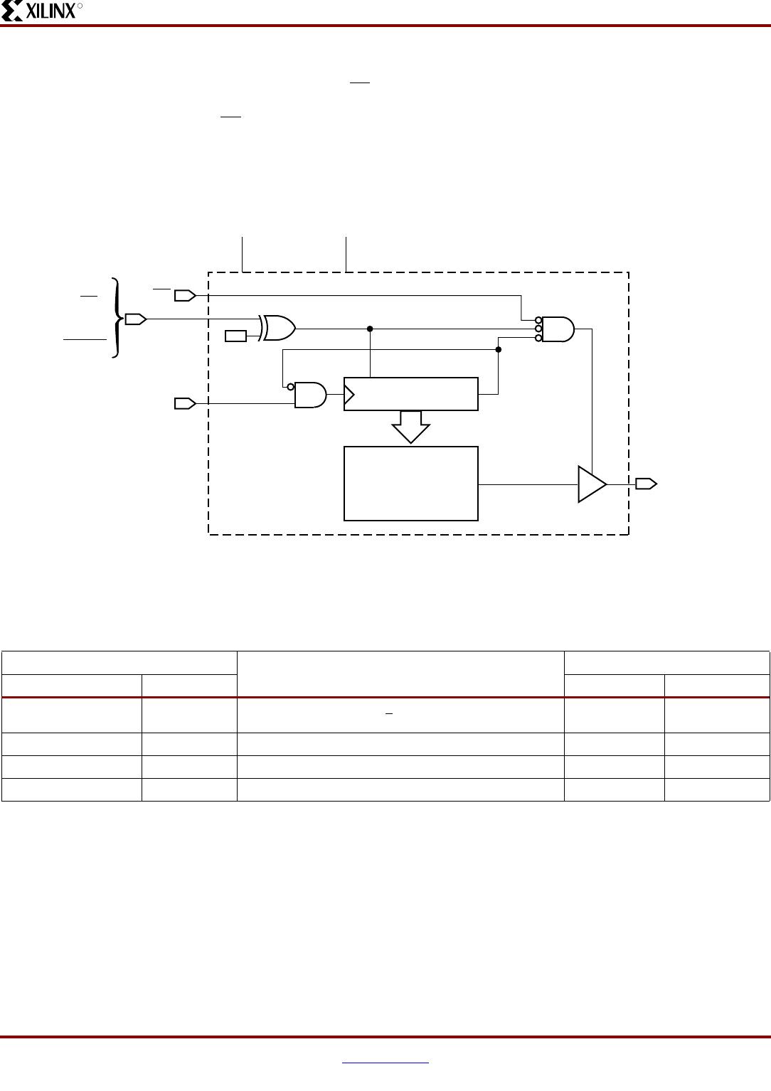
Spartan-II/Spartan-IIE Family OTP Configuration PROMs (XC17S00A)
DS078 (v1.10) June 25, 2007 www.xilinx.com
Product Specification 5
XC17S15A, XC17S30A, XC17S50A, XC17S100A, XC17S150A, XC17S200A, and
XC17S300A
Absolute Maximum Ratings
(1)
Operating Conditions
(1)
DC Characteristics Over Operating Condition
Symbol Description Value Units
V
CC
Supply voltage relative to GND –0.5 to +4.0 V
V
IN
Input voltage with respect to GND –0.5 to V
CC
+0.5 V
V
TS
Voltage applied to High-Z output –0.5 to V
CC
+0.5 V
T
STG
Storage temperature (ambient) –65 to +150 ° C
Notes:
1. Stresses beyond those listed under Absolute Maximum Ratings might cause permanent damage to the device. These are stress ratings only,
and functional operation of the device at these or any other conditions beyond those listed under Operating Conditions is not implied.
Exposure to Absolute Maximum Ratings conditions for extended periods of time might affect device reliability.
Symbol Description Min Max Units
V
CC
Commercial Supply voltage relative to GND (T
A
= 0° C to +70° C) 3.0 3.6 V
Industrial Supply voltage relative to GND (T
A
= –40° C to +85° C) 3.0 3.6 V
T
VCC
V
CC
rise time from 0V to nominal voltage 1.0 50 ms
Notes:
1. During normal read operation, both V
CC
pins must be connected together.
2. At power-up, the device requires the V
CC
power supply to monotonically rise from 0V to nominal voltage within the specified V
CC
rise time.
If the power supply cannot meet this requirement, then the device may not perform a power-on-reset properly.
Symbol Description Min Max Units
V
IH
High-level input voltage 2.0 V
CC
V
V
IL
Low-level input voltage 0 0.8 V
V
OH
High-level output voltage (I
OH
= –3 mA) 2.4 – V
V
OL
Low-level output voltage (I
OL
= +3 mA) – 0.4 V
I
CCA
Supply current, active mode (at maximum frequency) – 15 mA
I
CCS
Supply current, standby mode – 1 mΑ
I
L
Input or output leakage current –10 10 μA
C
IN
Input Capacitance (V
IN
= GND, f = 1.0 MHz) – 10 pF
C
OUT
Output Capacitance (V
IN
= GND, f = 1.0 MHz) – 10 pF