DS078 (v1.10) June 25, 2007 www.xilinx.com
Product Specification 1
© 2000-2002, 2005, 2007 Xilinx, Inc. All rights reserved. All Xilinx trademarks, registered trademarks, patents, and disclaimers are as listed at http://www.xilinx.com/legal.htm.
PowerPC is a trademark of IBM, Inc. All other trademarks are the property of their respective owners. All specifications are subject to change without notice.
Features
• Configuration one-time programmable (OTP) read-only
memory designed to store configuration bitstreams for
Spartan™-II/Spartan-IIE FPGA devices
• Simple interface to the Spartan device
• Programmable reset polarity (active High or active Low)
• Low-power CMOS floating gate process
• 3.3V PROM
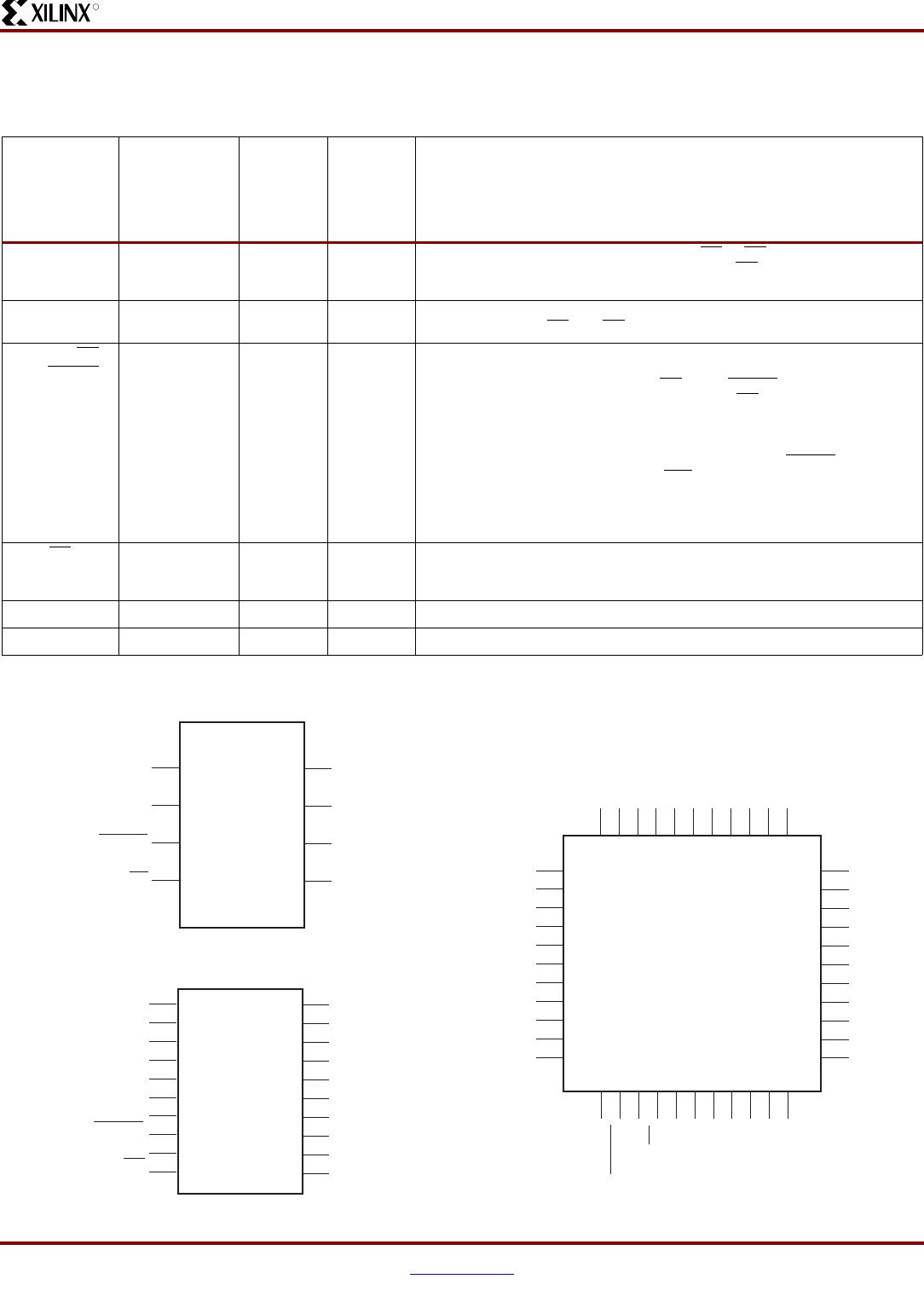
• Available in compact plastic 8-pin DIP, 8-pin VOIC,
20-pin SOIC, or 44-pin VQFP packages
• Programming support by leading programmer
manufacturers
• Design support using the Xilinx Alliance and
Foundation™ series software packages
• Guaranteed 20-year life data retention
• Pb-free (RoHS-compliant) packaging available
Introduction
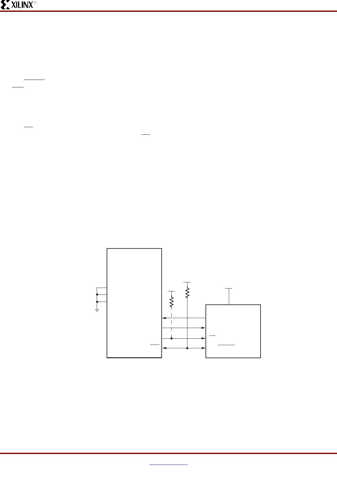
The XC17S00A family of PROMs provide an easy-to-use,
cost-effective method for storing Spartan-II/Spartan-IIE
device configuration bitstreams.
When the Spartan device is in Master Serial mode, it
generates a configuration clock that drives the Spartan
PROM. A short access time after the rising clock edge, data
appears on the PROM DATA output pin that is connected to
the Spartan device D
IN
pin. The Spartan device generates
the appropriate number of clock pulses to complete the
configuration. Once configured, it disables the PROM.
When a Spartan device is in Slave Serial mode, the PROM
and the Spartan device must both be clocked by an
incoming signal.
For device programming, either the Xilinx Alliance or the
Spartan device design file into a standard HEX format which
is then transferred to most commercial PROM programmers.
0
Spartan-II/Spartan-IIE Family OTP
Configuration PROMs (XC17S00A)
DS078 (v1.10) June 25, 2007
05
Product Specification
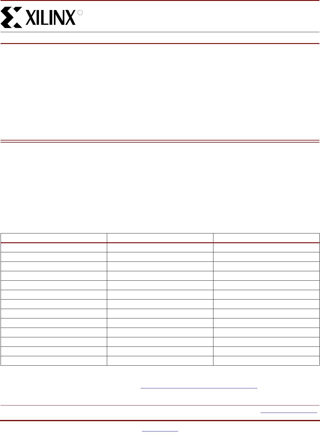
Spartan-II/IIE FPGA Configuration Bits Compatible Spartan-II/IIE PROM
XC2S15 197,696 XC17S15A
XC2S30 336,768 XC17S30A
XC2S50 559,200 XC17S50A
XC2S100 781,216 XC17S100A
XC2S150 1,040,096 XC17S150A
XC2S200 1,335,840 XC17S200A
XC2S50E 630,048 XC17S50A
XC2S100E 863,840 XC17S100A
XC2S150E
(1)
1,134,496 XC17S200A
XC2S200E 1,442,016 XC17S200A
XC2S300E 1,875,648 XC17S300A
XC2S400E 2,693,440 XC17V04
(2)
XC2S600E 3,961,632 XC17V04
(2)
Notes:
1. Due to the higher configuration bit requirements of the XC2S150E device, an XC17S200A PROM is required to configure this FPGA.
2. See XC17V00 series configuration PROMs data sheet at: http://direct.xilinx.com/bvdocs/publications/ds073.pdf