AD629
Rev. C | Page 4 of 16
ABSOLUTE MAXIMUM RATINGS
Table 2.
Parameter Rating
Supply Voltage, V
S
±18 V
Internal Power Dissipation
1
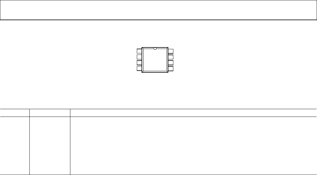
8-Lead PDIP (N) See Figure 4
8-Lead SOIC (R) See Figure 4
Input Voltage Range, Continuous ±300 V
Common-Mode and Differential, 10 sec ±500 V
Output Short-Circuit Duration Indefinite
Pin 1 and Pin 5 –V
S
− 0.3 V to +V
S
+ 0.3 V
Maximum Junction Temperature 150°C
Operating Temperature Range −55°C to +125°C
Storage Temperature Range −65°C to +150°C
Lead Temperature (Soldering 60 sec) 300°C
1
Specification is for device in free air:
8-Lead PDIP, θ
JA
= 100°C/W;
8-Lead SOIC, θ
JA
= 155°C/W.
Stresses above those listed under Absolute Maximum Ratings
may cause permanent damage to the device. This is a stress
rating only; functional operation of the device at these or any
other conditions above those indicated in the operational
section of this specification is not implied. Exposure to absolute
maximum rating conditions for extended periods may affect
device reliability.
AMBIENT TEMPERATURE (°C)
MAXIMUM POWER DISSIP
TION (W)
2.0
1.5
1.0
0.5
0
–50 –40 –30 –20 –10 0 10 20 30 40 50 60 70 80 90
00783-004
8-LEAD SOIC
T
J
= 150°C
8-LEAD PDIP
Figure 4. Maximum Power Dissipation vs. Temperature for SOIC and PDIP
DIE SIZE: 1655µm (X) by 2465µm (Y)
X
7
2
1a 1b
3
4
5a 5b
6b
6a
00783-041
Figure 5. Metallization Photograph
Table 3. Pin Pad Coordinates
Coordinates
1
Pad Pin X Y Description
1a REF(−) −677 +1082
1b −534 +1084
For the die model, either
pad can be bonded because
1a and 1b are internally
shorted.
2 −IN −661 +939
3 +IN −661 −658
4 −V
S
+680 −800
5a REF(+) +396 −1084
5b +538 −1084
For the die model, either
pad can be bonded because
5a and 5b are internally
shorted.
6a OUTPUT +681 −950
6b +681 −807
For the die model, both
pads must be bonded
because 6a and 6b are not
internally shorted.
7 +V
S
+680 +612
1
All coordinates are with respect to the center of the die.
ESD CAUTION