AD629
Rev. C | Page 12 of 16
ANALOG POWER
SUPPLY
DIGITAL
POWER SUPPLY
0.1µF
0.1µF
0.1µF0.1µF
+IN
–IN
–V
S
V
IN1
V
IN2
V
DD
V
DD
OUTPUT
AGND
GND
MICROPROCESSOR
DGND
+V
S
AD629
AD7892-2
REF(–) REF(+)
6
7
14
4
1
3
3
2
6 4
1 5
12
+5V GND
+5VGND
–5V
00783-032
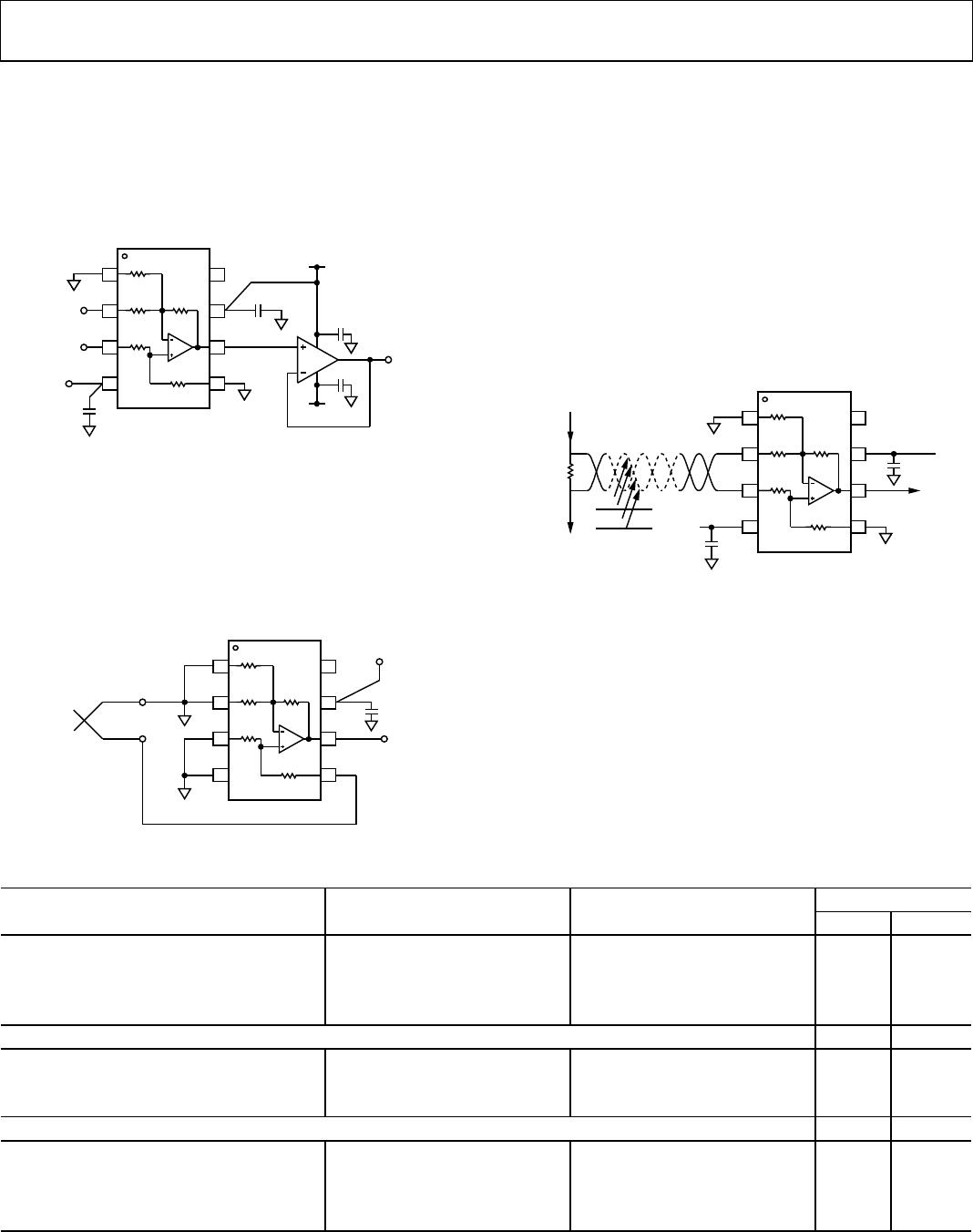
Figure 34. Optimal Grounding Practice for a Bipolar Supply Environment
with Separate Analog and Digital Supplies
POWER SUPPLY
V
IN1
V
IN2
V
DD
AGND DGND
ADC
0.1µF
0.1µF
+IN
–IN
+V
S
OUTPUT
–V
S
AD629
REF(–) REF(+)
47
3
2
6
1 5
V
DD
GND
MICROPROCESSOR
+5V
GND
0.1µF
00783-033
Figure 35. Optimal Ground Practice in a Single-Supply Environment
If there is only a single power supply available, it must be shared
by both digital and analog circuitry. Figure 35 shows how to
minimize interference between the digital and analog circuitry.
In this example, the ADC’s reference is used to drive Pin REF(+)
and Pin REF(–). This means that the reference must be capable
of sourcing and sinking a current equal to V
CM
/200 k. As in
the previous case, separate analog and digital ground planes
should be used (reasonably thick traces can be used as an
alternative to a digital ground plane). These ground planes
should connect at the power supply’s ground pin. Separate
traces (or power planes) should run from the power supply to
the supply pins of the digital and analog circuits. Ideally, each
device should have its own power supply trace, but these can be
shared by a number of devices, as long as a single trace is not
used to route current to both digital and analog circuitry.
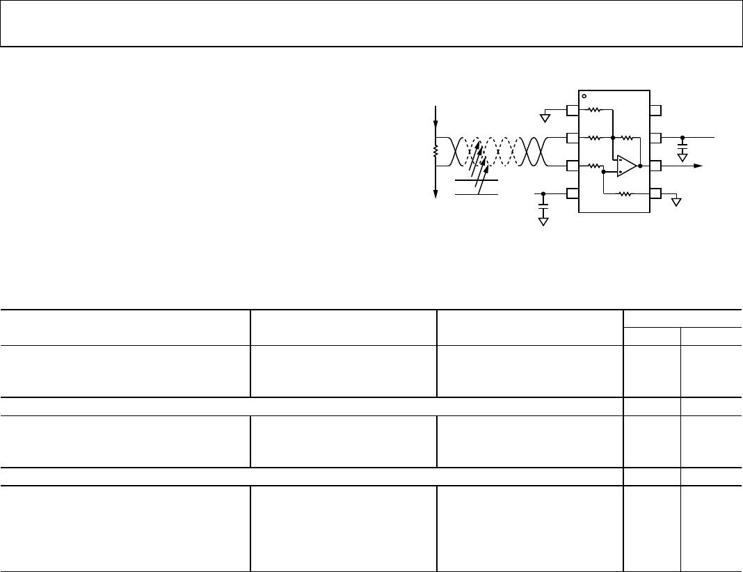
USING A LARGE SENSE RESISTOR
Insertion of a large value shunt resistance across the input pins,
Pin 2 and Pin 3, will imbalance the input resistor network,
introducing a common-mode error. The magnitude of the error
will depend on the common-mode voltage and the magnitude
of R
SHUNT
.
Tabl e 5 shows some sample error voltages generated by a
common-mode voltage of 200 V dc with shunt resistors from
20  to 2000 . Assuming that the shunt resistor is selected to
use the full ±10 V output swing of the AD629, the error voltage
becomes quite significant as R
SHUNT
increases.
Table 5. Error Resulting from Large Values of R
SHUNT
(Uncompensated Circuit)
R
S
(Ω) Error V
OUT
(V) Error Indicated (mA)
20 0.01 0.5
1000 0.498 0.498
2000 1 0.5
To measure low current or current near zero in a high common-
mode environment, an external resistor equal to the shunt
resistor value can be added to the low impedance side of the
shunt resistor, as shown in Figure 36.
REF (–)
REF (+)
–V
S
–V
S
+V
S
+V
S
V
OUT
NC
–IN
+IN
R
SHUNT
R
COMP
I
SHUNT
0.1µF
0.1µF
NC = NO CONNECT
21.1k
380k 380k
20k
380k
AD629
1
2
3
4
8
7
6
5
00783-034
Figure 36. Compensating for Large Sense Resistors
OUTPUT FILTERING
A simple 2-pole, low-pass Butterworth filter can be implemented
using the OP177 after the AD629 to limit noise at the output, as
shown in Figure 37. Table 6 gives recommended component
values for various corner frequencies, along with the peak-to-
peak output noise for each case.
REF (–)
REF (+)
V
S
–V
S
+V
S
+V
S
+V
S
V
OUT
NC
–IN
+IN
0.1µF
0.1µF 0.1µF
0.1µF
NC = NO CONNECT
21.1k
380k 380k
20k
380k
AD629
1
2
3
4
8
7
6
5
00783-035
R1 R2
C1
C2
OP177
Figure 37. Filtering of Output Noise Using a 2-Pole Butterworth Filter
Table 6. Recommended Values for 2-Pole Butterworth Filter
Corner Frequency R1 R2 C1 C2 Output Noise (p-p)
No Filter
3.2 mV
50 kHz 2.94 kΩ ± 1% 1.58 kΩ ± 1% 2.2 nF ± 10% 1 nF ± 10% 1 mV
5 kHz 2.94 kΩ ± 1% 1.58 kΩ ± 1% 22 nF ± 10% 10 nF ± 10% 0.32 mV
500 Hz 2.94 kΩ ± 1% 1.58 kΩ ± 1% 220 nF ± 10% 0.1 μF ± 10% 100 μV
50 Hz 2.7 kΩ ± 10% 1.5 kΩ ± 10% 2.2 μF ± 20% 1 μF ± 20% 32 μV
AD629
Rev. C | Page 13 of 16
OUTPUT CURRENT AND BUFFERING
The AD629 is designed to drive loads of 2 kΩ to within 2 V of
the rails but can deliver higher output currents at lower output
voltages (see Figure 17). If higher output current is required, the
output of the AD629 should be buffered with a precision op amp,
such as the OP113, as shown in Figure 38. This op amp can swing
to within 1 V of either rail while driving a load as small as 600 Ω.
REF (–)
REF (+)
V
S
–V
S
+V
S
V
OU
T
NC
–IN
+IN
0.1µF
0.1µF
0.1µF
0.1µF
NC = NO CONNECT
21.1k
380k 380k
20k
380k
AD629
1
2
3
4
8
7
6
5
00783-036
OP113
Figure 38. Output Buffering Application
A GAIN OF 19 DIFFERENTIAL AMPLIFIER
While low level signals can be connected directly to the –IN and
+IN inputs of the AD629, differential input signals can also be
connected, as shown in Figure 39, to give a precise gain of 19.
However, large common-mode voltages are no longer permissible.
Cold junction compensation can be implemented using a
temperature sensor, such as the AD590.
REF (–)
REF (+)
+V
S
+V
S
NC
–IN
+IN
0.1µF
NC = NO CONNECT
21.1k
380k 380k
20k
380k
AD629
1
2
3
4
8
7
6
5
00783-037
V
OU
V
REF
THERMOCOUPLE
Figure 39. A Gain of 19 Thermocouple Amplifier
ERROR BUDGET ANALYSIS EXAMPLE 1
In the dc application that follows, the 10 A output current from
a device with a high common-mode voltage (such as a power
supply or current-mode amplifier) is sensed across a 1 Ω shunt
resistor (see Figure 40). The common-mode voltage is 200 V,
and the resistor terminals are connected through a long pair of
lead wires located in a high noise environment, for example,
50 Hz/60 Hz, 440 V ac power lines. The calculations in Table 7
assume an induced noise level of 1 V at 60 Hz on the leads, in
addition to a full-scale dc differential voltage of 10 V. The error
budget table quantifies the contribution of each error source.
Note that the dominant error source in this example is due to
the dc common-mode voltage.
REF (–)
OUTPUT
CURRENT
60Hz
POWER LINE
1
SHUNT
REF (+)
–V
S
+V
S
V
OUT
NC
–IN
+IN
0.1µF
0.1µF
NC = NO CONNECT
21.1k
380k 380k
20k
380k
AD629
1
2
3
4
8
7
6
5
00783-038
10 AMPS
200V
CM
DC
TO GROUND
Figure 40. Error Budget Analysis Example 1: V
IN
= 10 V Full-Scale,
V
CM
= 200 V DC, R
SHUNT
= 1 Ω, 1 V p-p, 60 Hz Power-Line Interference
Table 7. AD629 vs. INA117 Error Budget Analysis Example 1 (V
CM
= 200 V dc)
Error, ppm of FS
Error Source AD629 INA117 AD629 INA117
ACCURACY, T
A
= 25°C
Initial Gain Error (0.0005 × 10)/10 V × 10
6
(0.0005 × 10)/10 V × 10
6
500 500
Offset Voltage (0.001 V/10 V) × 10
6
(0.002 V/10 V) × 10
6
100 200
DC CMR (Over Temperature) (224 × 10
-6
× 200 V)/10 V × 10
6
(500 × 10
-6
× 200 V)/10 V × 10
6
4480 10,000
Total Accuracy Error
5080 10,700
TEMPERATURE DRIFT (85°C)
Gain 10 ppm/°C × 60°C 10 ppm/°C × 60°C 600 600
Offset Voltage (20 μV/°C × 60°C) × 10
6
/10 V (40 μV/°C × 60°C) × 10
6
/10 V 120 240
Total Drift Error
720 840
RESOLUTION
Noise, Typical, 0.01 Hz to 10 Hz, μV p-p 15 μV/10 V × 10
6
25 μV/10 V × 10
6
2 3
CMR, 60 Hz (141 × 10
-6
× 1 V)/10 V × 10
6
(500 × 10
-6
× 1 V)/10 V × 10
6
14 50
Nonlinearity (10
-5
× 10 V)/10 V × 10
6
(10
-5
× 10 V)/10 V × 10
6
10 10
Total Resolution Error
26 63
Total Error
5826 11,603
AD629
Rev. C | Page 14 of 16
ERROR BUDGET ANALYSIS EXAMPLE 2
This application is similar to the previous example except
that the sensed load current is from an amplifier with an ac
common-mode component of ±100 V (frequency = 500 Hz)
present on the shunt (see Figure 41). All other conditions are
the same as before. Note that the same kind of power-line
interference can happen as detailed in Example 1. However,
the ac common-mode component of 200 V p-p coming from
the shunt is much larger than the interference of 1 V p-p;
therefore, this interference component can be neglected.
REF (–)
OUTPUT
CURRENT
60Hz
POWER LINE
1
SHUNT
REF (+)
–V
S
+V
S
V
OUT
NC
–IN
+IN
0.1µF
0.1µF
NC = NO CONNECT
21.1k
380k 380k
20k
380k
AD629
1
2
3
4
8
7
6
5
00783-039
10 AMPS
±100V AC CM
TO GROUND
Figure 41. Error Budget Analysis Example 2: V
IN
= 10 V Full-Scale,
V
CM
= ±100 V at 500 Hz, R
SHUNT
=1 Ω
Table 8. AD629 vs. INA117 AC Error Budget Example 2 (V
CM
= ±100 V @ 500 Hz)
Error, ppm of FS
Error Source AD629 INA117 AD629 INA117
ACCURACY, T
A
= 25°C
Initial Gain Error (0.0005 × 10)/10 V × 10
6
(0.0005 × 10)/10 V × 10
6
500 500
Offset Voltage (0.001 V/10 V) × 10
6
(0.002 V/10 V) × 10
6
100 200
Total Accuracy Error
600 700
TEMPERATURE DRIFT (85°C)
Gain 10 ppm/°C × 60°C 10 ppm/°C × 60°C 600 600
Offset Voltage (20 μV/°C × 60°C) × 10
6
/10 V (40 μV/°C × 60°C) × 10
6
/10 V 120 240
Total Drift Error
720 840
RESOLUTION
Noise, Typical, 0.01 Hz to 10 Hz, μV p-p 15 μV/10 V × 10
6
25 μV/10 V × 10
6
2 3
CMR, 60 Hz (141 × 10
-6
× 1 V)/10 V × 10
6
(500 × 10
-6
× 1 V)/10 V × 10
6
14 50
Nonlinearity (10
-5
× 10 V)/10 V × 10
6
(10
-5
× 10 V)/10 V × 10
6
10 10
AC CMR @ 500 Hz (141 × 10
-6
× 200 V)/10 V × 10
6
(500 × 10
-6
× 200 V)/10 V × 10
6
2820 10,000
Total Resolution Error
2846 10,063
Total Error
4166 11,603

AD629BR

Mfr. #:
Manufacturer:
Analog Devices Inc.
Description:
Differential Amplifiers High CM Vltg
Lifecycle:
New from this manufacturer.
Delivery:
DHL FedEx Ups TNT EMS
Payment:
T/T Paypal Visa MoneyGram Western Union