©2015 Fairchild Semiconductor Corporation www.fairchildsemi.com
FOD8163, FOD8163T Rev. 1.1 4
FOD8163, FOD8163T — 3.3 V / 5 V, 10 Mbit/sec, Logic Gate Optocoupler in Stretched Body SOP 6-Pin
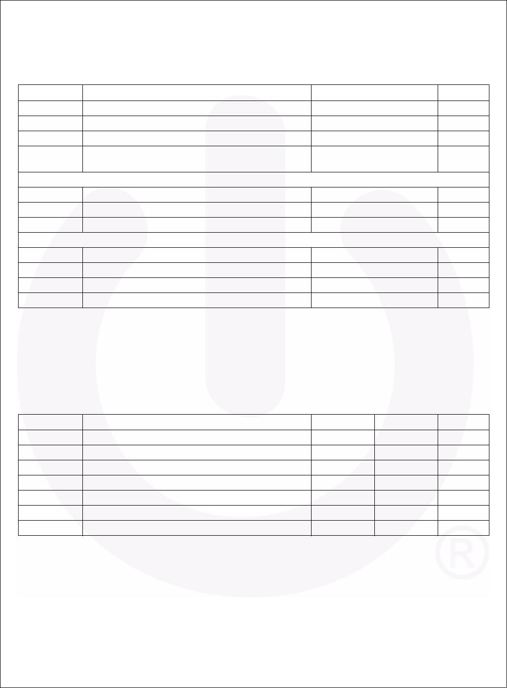
Absolute Maximum Ratings
Stresses exceeding the absolute maximum ratings may damage the device. The device may not function or be
operable above the recommended operating conditions and stressing the parts to these levels is not recommended.
In addition, extended exposure to stresses above the recommended operating conditions may affect device reliability.
The absolute maximum ratings are stress ratings only. T
A
= 25°C unless otherwise specified.
Note:
1. No derating required up to 100°C.
Recommended Operating Conditions
The Recommended Operating Conditions table defines the conditions for actual device operation. Recommended
operating conditions are specified to ensure optimal performance to the datasheet specifications. Fairchild does not
recommend exceeding them or designing to absolute maximum ratings.
Note:
2. 0.1 F bypass capacitor must be connected between pins 4 and 6.
Symbol Parameter Value Unit
T
STG
Storage Temperature -40 to +125 °C
T
OPR
Operating Temperature -40 to +100 °C
T
J
Junction Temperature -40 to +125 °C
T
SOL
Lead Solder Temperature
(Refer to Reflow Temperature Profile)
260 for 10 sec °C
Input Characteristics
I
F
Average Forward Input Current 25 mA
V
R
Reverse Input Voltage 5.0 V
PD
I
Input Power Dissipation
(1)
45 mW
Output Characteristics
V
CC
Supply Voltage 0 to 7.0 V
V
O
Output Voltage -0.5 to V
CC
+ 0.5 V
I
O
Average Output Current 50 mA
PD
O
Output Power Dissipation
(1)
85 mW
Symbol Parameter Min. Max. Unit
T
A
Ambient Operating Temperature -40 +100 ºC
V
CC
Supply Voltages
(2)
3.0 5.5 V
V
FL
Logic Low Input Voltage 0 0.8 V
I
FL
Logic Low Input Current 250 A
I
FH
Logic High Input Current 6.0 15 mA
N Fan Out (at R
L
= 1 k) 5 TTL loads
R
L
Output Pull-up Resistor 330 4000

