MAX7306/MAX7307
SMBus/I
2
C Interfaced 4-Port, Level-Translating
GPIOs and LED Drivers
_______________________________________________________________________________________ 7
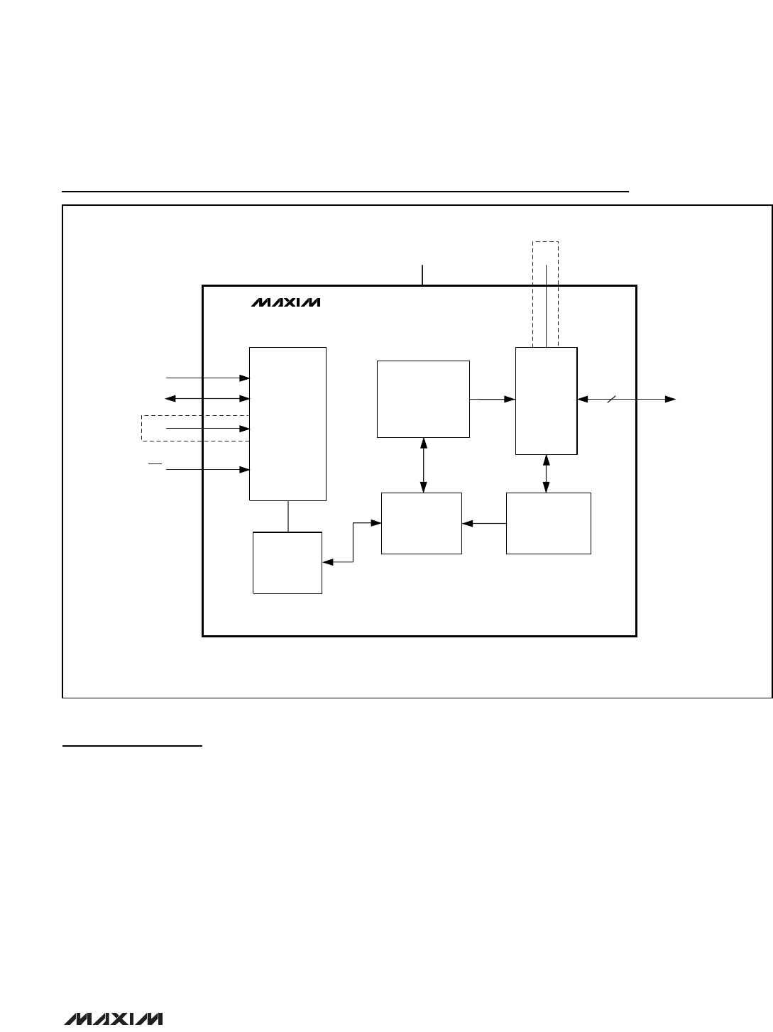
Detailed Description
The MAX7306/MAX7307 4-port, general-purpose port
expanders operate from a 1.62V to 3.6V power supply.
Ports P2 through P4 can be configured as inputs, push-
pull outputs, and open-drain outputs. Port P1 can be
configured as an input and an open-drain output; P1
can also be configured to function as an (INT) output.
Each port configured as an open-drain or push-pull
output can sink up to 25mA. Push-pull outputs also
have a 10mA source drive capability. The MAX7306/
MAX7307 are rated to sink a total of 100mA into any
combination of the output ports. Output ports have
PWM and blink capabilities, as well as logic drive.
Initial Power-Up
On power-up, the MAX7307 default configuration has
all ports configured as input ports with logic levels ref-
erenced to V
LA
. The MAX7306 default configuration
has all ports configured as input ports with logic levels
referenced to V
DD
. The transition detection interrupt
status flag resets and stays high (see Tables 1 and 2).
Device Configuration Registers
The device configuration registers set up the interrupt
function, serial-interface bus timeout, PWM/blink, oscil-
lator options, global blink period, and reset options
(see Tables 3 and 4).
I
2
C
OUTPUT
LOGIC
I/O
P1–P4
I/O
CONTROL
REGISTER
BANK
MAX7307 ONLY
INPUT
LOGIC
SDA
SCL
MAX7306 ONLY
V
LA
V
DD
AD0
RST
MAX7306/
MAX7307
Block Diagram
MAX7306/MAX7307
SMBus/I
2
C Interfaced 4-Port, Level-Translating
GPIOs and LED Drivers
8 _______________________________________________________________________________________
REGISTER DATA
REGISTER POWER-UP CONDITION
ADDRESS
CODE (hex)
D7 D6 D5 D4 D3 D2 D1 D0
Ports P1–P4
Ports P_ are V
LA
referred input ports with interrupt
and debounce disabled
0x01–0x04 1 0 0 0 0 0 0 0
Configuration 26
RST d oes not r eset r eg i ster s or counters; b l i nk p er i od
i s 1H z; tr ansi ti on fl ag cl ear ; i nterr up t status fl ag cl ear
0x26 1 1 1 0 1 1 0 0
Configuration 27
Ports P1–P4 are GPIO ports; bus timeout is
disabled
0x27 1 0 0 0 1 1 1 1
Table 2. Power-Up Register Status
REGISTER ADDRESS
AUTOINCREMENT ADDRESS
POR STATE
Port P1 or INT Output 0x01 0x02 0x80
Port P2 or OSCIN Input 0x02 0x03 0x80
Port P3 or OSCOUT Output 0x03 0x04 0x80
Port P4 0x04 0x05* 0x80
Configuration 26 0x26 0x27 0xEC
Configuration 27 0x27 0x28* 0x8F
FACTORY RESERVED (Do not write to these registers) 0x3C–0x3F 0x3F–0x40 0x00
FACTORY RESERVED (Do not write to these registers) 0x00 0x01 0x80
Table 1. Register Address Map
*No registers are present.
MAX7306/MAX7307
SMBus/I
2
C Interfaced 4-Port, Level-Translating
GPIOs and LED Drivers
_______________________________________________________________________________________ 9
REGISTER BIT DESCRIPTION VALUE FUNCTION
0 An interrupt has occurred on at least one interrupt enabled input port.
D7
Interrupt Status
Flag (Read-Only)
1* No interrupt has occurred on an interrupt enabled input port.
0 Transition has occurred on an input port.
D6
Transition Flag
(Read-Only)
1* No transition has occurred on an input port.
D5 Reserved 0 Reserved.
D4, D3, D2
Blink Prescaler Bits
0/1 See Table 9 for blink frequency setting.
0* RST does not reset PWM/blink counters.
D1 RST Timer
1 RST resets PWM/blink counters.
0* RST does not reset registers to power-on-reset state.
D0 RST POR
1 RST resets registers to power-on-reset state.
Table 3. Configuration Register (0x26)
*Default state.
REGISTER BIT DESCRIPTION
VALUE
FUNCTION
0 Enables the bus timeout feature.
D7 Bus Timeout
1* Disables the bus timeout feature.
D6, D5, D4 Reserved 0 Reserved.
0 Sets P3 to output the oscillator.
D3 P3/OSCOUT
1* Sets P3 as a GPIO controlled by register 0x03.
0 Sets P2 as the oscillator input.
D2 P2/OSCIN
1* Sets P2 as a GPIO controlled by register 0x02.
0 Sets P1 as the interrupt output.
D1 P1/INT Output
1* Sets P1 as a GPIO controlled by register 0x01.
D0 Input Transition 0 Set to 0 on power-up for proper transition detection.
Table 4. Configuration Register (0x27)
*Default state.

MAX7307AUB+

Mfr. #:
Manufacturer:
Maxim Integrated
Description:
Interface - I/O Expanders 4-Port Level-Trans GPIO & LED Driver
Lifecycle:
New from this manufacturer.
Delivery:
DHL FedEx Ups TNT EMS
Payment:
T/T Paypal Visa MoneyGram Western Union

Products related to this Datasheet