8Mb
SMART 3 BOOT BLOCK FLASH MEMORY
09005aef81136a91 Micron Technology, Inc., reserves the right to change products or specifications without notice.
Q10.fm - Rev. E 6/04 EN
13 ©2001 Micron Technology, Inc. All rights reserved.
ERASE Sequence
Executing an ERASE sequence sets all bits within a
block to logic 1. The command sequence necessary to
execute an ERASE is similar to that of a WRITE. To pro-
vide added security against accidental block erasure,
two consecutive command cycles are required to ini-
tiate an ERASE of a block. In the first cycle, addresses
are “Don’t Care,” and ERASE SETUP (20h) is given. In
the second cycle, V
PP must be brought to VPPH, an
address within the block to be erased must be issued,
and ERASE CONFIRM (D0h) must be given. If a com-
mand other than ERASE CONFIRM is given, the write
and erase status bits (SR4 and SR5) are set, and the
device is in the status register read mode.
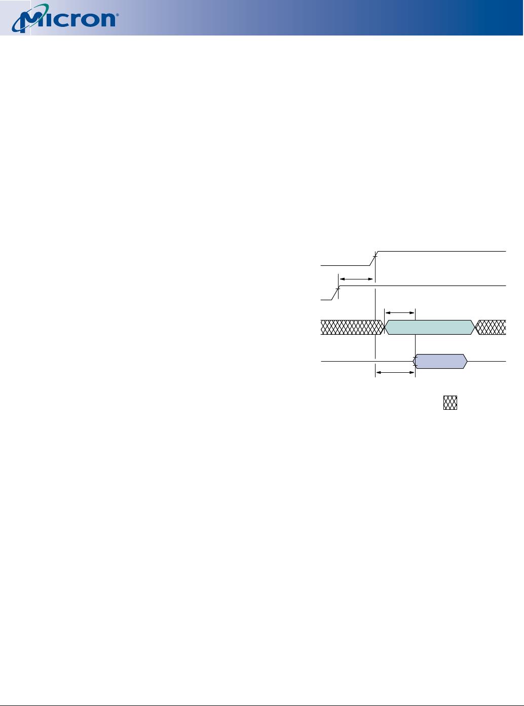
After the ERASE CONFIRM (D0h) is issued, the ISM
starts the ERASE of the addressed block. Any READ
operation outputs the status register contents on
DQ0–DQ7. V
PP must be held at VPPH until the ERASE is
completed (SR7 = 1). When the ERASE is completed,
the device is in the status register read mode until
another command is issued. Erasing the boot block
also requires that either the RP# pin be set to V
HH or
the WP# pin be held HIGH at the same time V
PP is set
to V
PPH.
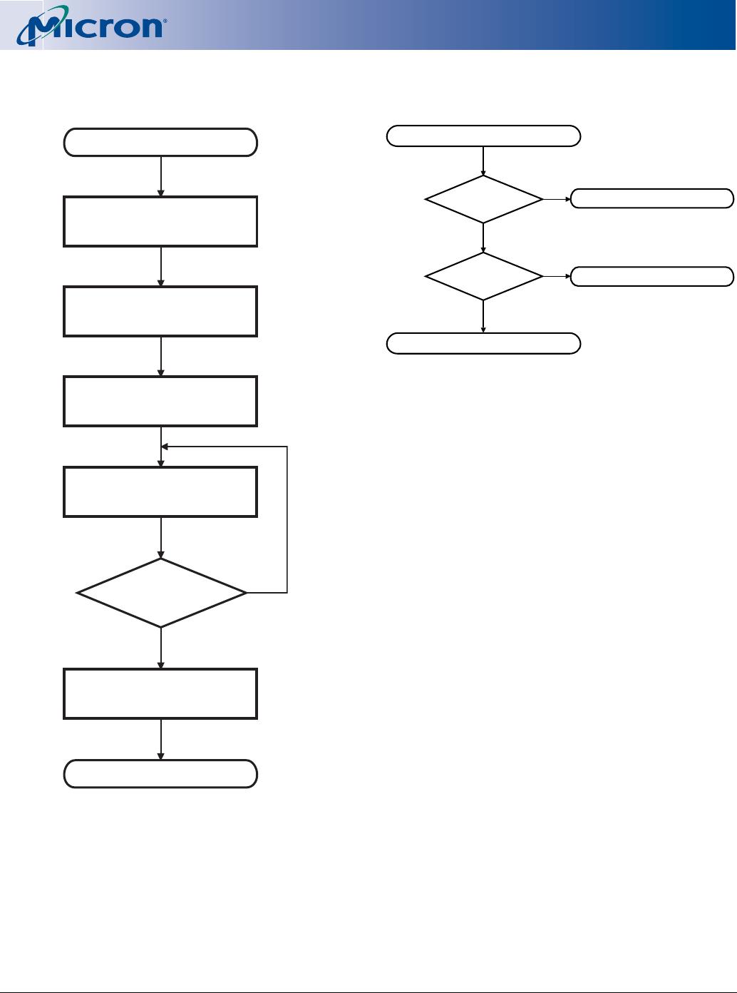
ERASE Suspension
The only command that may be issued while an
ERASE is in progress is ERASE SUSPEND. This com-
mand enables other commands to be executed while
pausing the ERASE in progress. When the device has
reached the erase suspend mode, the erase suspend
status bit (SR6) and ISM status bit (SR7) are set. The
device may now be given a READ ARRAY, ERASE
RESUME or READ STATUS REGISTER command. After
READ ARRAY has been issued, any location not within
the block being erased may be read. If ERASE RESUME
is issued before SR6 has been set, the device immedi-
ately proceeds with the ERASE in progress.
Error Handling
After the ISM status bit (SR7) has been set, the VPP
(SR3), write (SR4) and erase (SR5) status bits may be
checked. If one or a combination of these three bits
has been set, an error has occurred. The ISM cannot
reset these three bits. To clear these bits, CLEAR STA-
TUS REGISTER (50h) must be given. If the V
PP status
bit (SR3) is set, further WRITE or ERASE operations
cannot resume until the status register is cleared.
Table 7 lists the combination of errors.
NOTE:
1. SR3–SR5 must be cleared using CLEAR STATUS REGISTER.
Table 7: Status Register Error Code Description
1
STATUS BITS
ERROR DESCRIPTIONSR5 SR4 SR3
000
No errors
001
V
PP voltage error
010
WRITE error
011
WRITE error, V
PP voltage not valid at time of WRITE
100
ERASE error
101
ERASE error, V
PP voltage not valid at time of ERASE CONFIRM
110
Command sequencing error or WRITE/ERASE error
111
Command sequencing error, V
PP voltage error, with WRITE and ERASE errors