2305NZ-1HDCGI

1
COMMERCIAL AND INDUSTRIAL TEMPERATURE RANGES
IDT2305NZ
FIVE OUTPUT 3.3V CLOCK BUFFER
FEB. 2017
2017Integrated Device Technology, Inc. DSC 6592/5c
COMMERCIAL AND INDUSTRIAL TEMPERATURE RANGES
The IDT logo is a registered trademark of Integrated Device Technology, Inc.
FEATURES:
One input to five output buffer/driver
Low power consumption for mobile applications: less than
32mA at 66.6MHz with unloaded outputs
8.7ns max input-output delay
Buffers all frequencies from DC to 133.33MHz
Output-output skew < 250ps
3.3V operation
High drive capability
Available in SOIC package
FUNCTIONAL BLOCK DIAGRAM
IDT2305NZ
FIVE OUTPUT
3.3V CLOCK BUFFER
DESCRIPTION:
The IDT2305NZ is a low-cost buffer designed to distribute high-speed
clocks in mobile PC systems and desktop PC systems. The IDT2305NZ
operates at 3.3V with five outputs that can run up to 133.33MHz
The IDT2305NZ is an 8-pin version of the IDT2309NZ. It is designed
for low EMI and power optimization and consumes less than 32mA at
66.6MHz, making it ideal for the low power requirements of mobile systems.
OUTPU T2
OUTPUT3
OUTPUT4
OUTPUT1
BUF_IN
OUTPUT5
2
COMMERCIAL AND INDUSTRIAL TEMPERATURE RANGES
IDT2305NZ
FIVE OUTPUT 3.3V CLOCK BUFFER
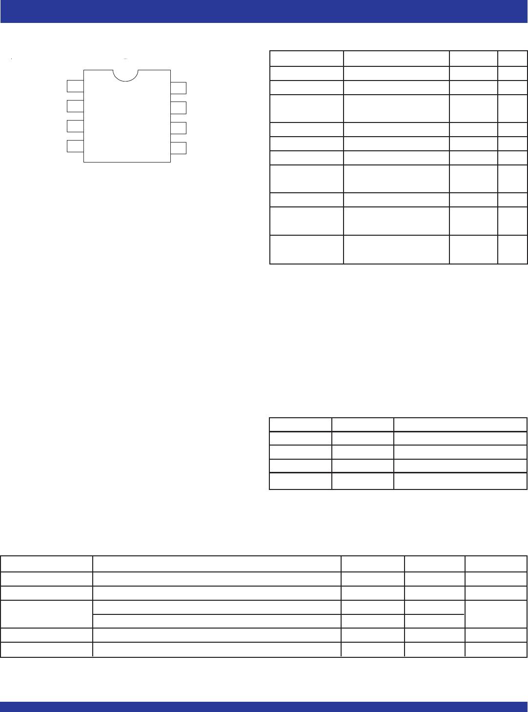
PIN CONFIGURATION
SOIC
TOP VIEW
PIN DESCRIPTION
Pin Name Pin Number Functional Description
VDD 6 3.3V Digital Voltage Supply
GND 4 Ground
BUF_IN 1 Input clock
OUTPUT
[1:5] 2, 3, 6, 7, 10 Outputs
Symbol Parameter Min. Max. Unit
VDD Supply Voltage 3 3.6 V
TA Operating Temperature (Ambient Temperature) 0 70 °C
CL Load Capacitance, FOUT < 100MHz 30 pF
Load Capacitance 100MHz < FOUT < 133.33MHz 15
CIN Input Capacitance 7 pF
BUF_IN, OUTPUT[1:5] Operating Frequency D C 133.33 MHz
OPERATING CONDITIONS - COMMERCIAL
Symbol Rating Max. Unit
VDD Supply Voltage Range –0.5 to +4.6 V
VI
(2)
Input Voltage Range (REF) –0.5 to +5.5 V
V
I Input Voltage Range –0.5 to V
(except REF) VDD+0.5
IIK (VI < 0) Input Clamp Current 50 mA
IO (VO = 0 to VDD) Continuous Output Current ±50 mA
VDD or GND Continuous Current ±100 mA
T
A = 55°C Maximum Power Dissipation 0.7 W
(in still air)
(3)
TSTG Storage Temperature Range –65 to +150 ° C
Operating Commercial Temperature 0 to +70 °C
Temperature Range
Operating Industrial Temperature -40 to +85 °C
Temperature Range
NOTES:
1. Stresses greater than those listed under ABSOLUTE MAXIMUM RATINGS may cause
permanent damage to the device. This is a stress rating only and functional operation
of the device at these or any other conditions above those indicated in the operational
sections of this specification is not implied. Exposure to absolute maximum rating
conditions for extended periods may affect reliability.
2. The input and output negative-voltage ratings may be exceeded if the input and output
clamp-current ratings are observed.
3. The maximum package power dissipation is calculated using a junction temperature
of 150°C and a board trace length of 750 mils.
ABSOLUTE MAXIMUM RATINGS
(1)
BUF_IN
OUTPUT1
2
3
4
5
6
7
8
1
OUTPUT2
OUTPUT5
OUTPUT4
OUTPUT3
GND
V
DD
3
COMMERCIAL AND INDUSTRIAL TEMPERATURE RANGES
IDT2305NZ
FIVE OUTPUT 3.3V CLOCK BUFFER
SWITCHING CHARACTERISTICS - COMMERCIAL
(1)
Symbol Parameter
(2)
Conditions Min. Typ. Max. Unit
t3 Rise Time Measured between 0.8V and 2V 1.5 ns
t4 Fall Time Measured between 0.8V and 2V 1.5 ns
t5 Output to Output Skew All outputs equally loaded 250 ps
t6 Propagation Delay, BUF_IN Rising Edge Measured at VDD/2 1 5 8.7 ns
to OUTPUT Rising Edge
DC Duty Cycle Measured at V
DD/2 45 55 %
NOTES:
1. All parameters specified with loaded outputs.
2. Parameter is guaranteed by design but not production tested.
DC ELECTRICAL CHARACTERISTICS - INDUSTRIAL
Symbol Parameter Conditions Min. Max. Unit
VIL Input LOW Voltage
(1)
0.8 V
VIH Input HIGH Voltage
(1)
2—V
IIL Input LOW Current VIN = 0V 50 μA
IIH Input HIGH Current VIN = VDD —100μA
VOL Output LOW Voltage
(2)
IOL = 12mA 0.4 V
VOH Output HIGH Voltage
(2)
IOH = -12mA 2.4 V
IDD Supply Current Unloaded Outputs at 66.66MHz 35 mA
NOTES:
1. BUF_IN input has a threshold voltage of VDD/2.
2. Parameter is guaranteed by design but not production tested.
Symbol Parameter Min. Max. Unit
VDD Supply Voltage 3 3.6 V
TA Operating Temperature (Ambient Temperature) -40 +85 °C
CL Load Capacitance, FOUT < 100MHz 30 pF
Load Capacitance 100MHz < FOUT < 133.33MHz 15
CIN Input Capacitance 7 pF
BUF_IN, OUTPUT[1:5] Operating Frequency D C 133.33 MHz
OPERATING CONDITIONS - INDUSTRIAL
DC ELECTRICAL CHARACTERISTICS - COMMERCIAL
Symbol Parameter Conditions Min. Max. Unit
VIL Input LOW Voltage
(1)
0.8 V
VIH Input HIGH Voltage
(1)
2—V
IIL Input LOW Current VIN = 0V 50 μA
IIH Input HIGH Current VIN = VDD —100μA
VOL Output LOW Voltage
(2)
IOL = 12mA 0.4 V
VOH Output HIGH Voltage
(2)
IOH = -12mA 2.4 V
IDD Supply Current Unloaded Outputs at 66.66MHz 32 mA
NOTES:
1. BUF_IN input has a threshold voltage of VDD/2.
2. Parameter is guaranteed by design but not production tested.

2305NZ-1HDCGI

Mfr. #:
Manufacturer:
IDT
Description:
Clock Buffer Five Output 3.3V Clock Buff 133.33Mhz
Lifecycle:
New from this manufacturer.
Delivery:
DHL FedEx Ups TNT EMS
Payment:
T/T Paypal Visa MoneyGram Western Union

Products related to this Datasheet