LTC2605/LTC2615/LTC2625
1
2605fa
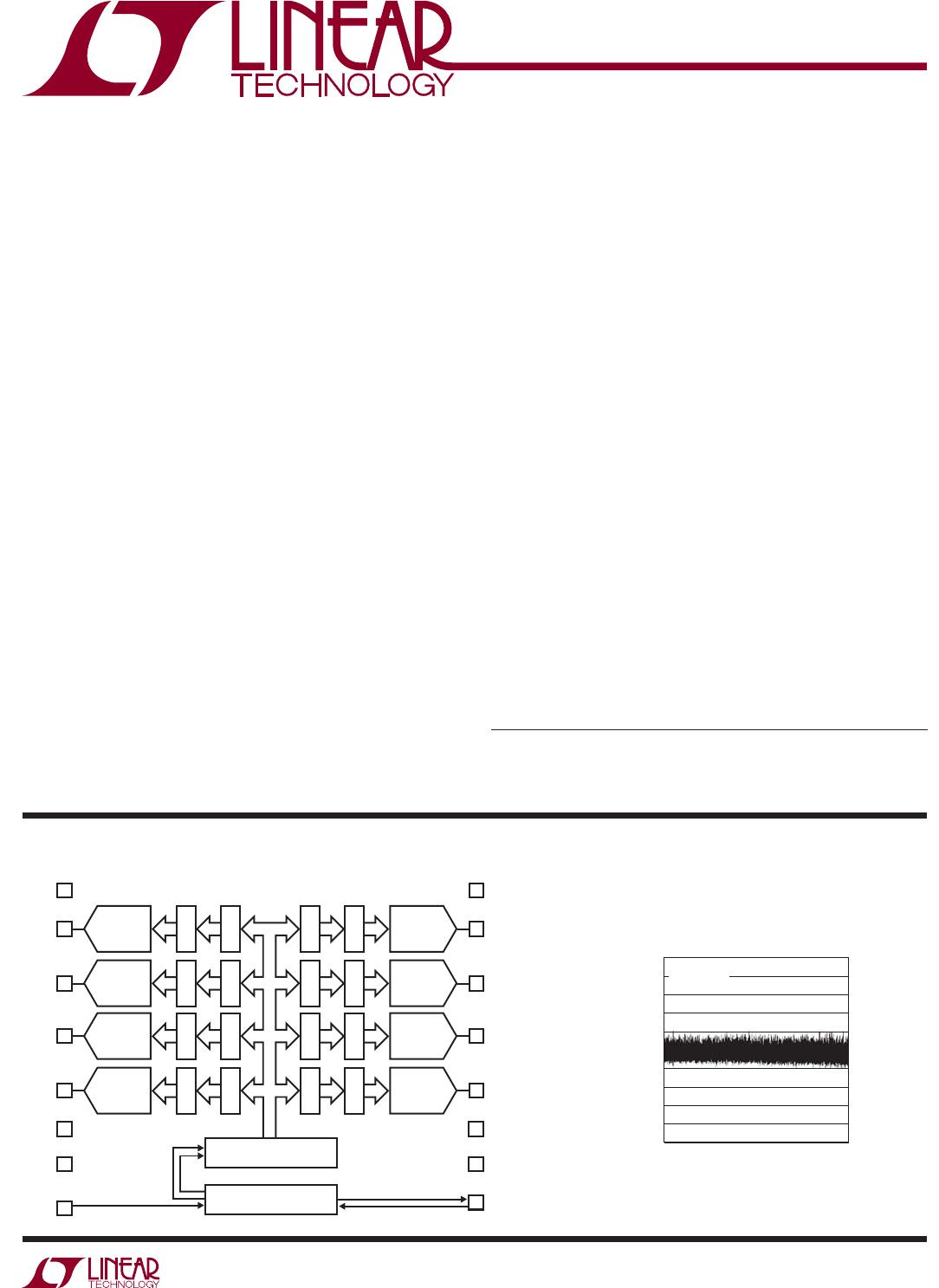
TYPICAL APPLICATION
FEATURES DESCRIPTION
Octal 16-/14-/12-Bit
Rail-to Rail DACs in 16-Lead SSOP
The LTC
®
2605/LTC2615/LTC2625 are octal 16-, 14- and
12-bit, 2.7V to 5.5V rail-to-rail voltage-output DACs
in 16-lead narrow SSOP packages. They have built-in
high performance output buffers and are guaranteed
monotonic.
These parts establish new board-density benchmarks
for 16-/14-bit DACs and advance performance standards
for output drive, crosstalk and load regulation in single
supply, voltage-output multiples.
The parts use the 2-wire I
2
C compatible serial interface. The
LTC2605/LTC2615/LTC2625 operate in both the standard
mode (maximum clock rate of 100kHz) and the fast mode
(maximum clock rate of 400kHz).
The LTC2605/LTC2615/LTC2625 incorporate a power-on
reset circuit. During power-up, the voltage outputs rise less
than 10mV above zero-scale; and after power-up, they stay
at zero-scale until a valid write and update take place. The
power-on reset circuit resets the LTC2605-1/\LTC2615-1/
LTC2625-1 to mid-scale. The voltage output stays at mid-
scale until a valid write and update takes place.
Differential Nonlinearity (LTC2605)
APPLICATIONS
n
Smallest Pin-Compatible Octal DACs:
LTC2605: 16 Bits
LTC2615: 14 Bits
LTC2625: 12 Bits
n
Guaranteed Monotonic Over Temperature
n
400kHz I
2
C Interface
n
Wide 2.7V to 5.5V Supply Range
n
Low Power Operation: 250μA per DAC at 3V
n
Individual Channel Power-Down to 1μA (Max)
n
Ultralow Crosstalk Between DACs (<10μV)
n
High Rail-to-Rail Output Drive (±15mA, Min)
n
Double-Buffered Digital Inputs
n
27 Selectable Addresses
n
LTC2605/LTC2615/LTC2625: Power-On Reset to
Zero-Scale
n
LTC2605-1/LTC2615-1/LTC2625-1: Power-On Reset
to Mid-Scale
n
Tiny 16-Lead Narrow SSOP Package
n
Mobile Communications
n
Process Control and Industrial Automation
n
Instrumentation
n
Automatic Test Equipment
L, LT, LTC, LTM, Linear Technology and the Linear logo are registered trademarks of Linear
Technology Corporation. All other trademarks are the property of their respective owners.
2
15
1GND
V
OUT A
V
OUT B
V
OUT C
V
OUT D
REF
CA2
SCL
V
CC
V
OUT H
V
OUT G
V
OUT F
V
OUT E
CA0
CA1
SDA
2605/15/25 BD
16
DAC A
3 14
4 13
5
7
6
8
10
11
9
12
2-WIRE INTERFACE
32-BIT SHIFT REGISTER
REGISTER
REGISTER
DAC H
REGISTER
REGISTER
DAC B
REGISTER
REGISTER
DAC G
REGISTER
REGISTER
DAC C
REGISTER
REGISTER
DAC F
REGISTER
REGISTER
DAC D
REGISTER
REGISTER
DAC E
REGISTER
REGISTER
CODE
0 16384 32768 49152 65535
DNL (LSB)
2605 G02
1.0
0.8
0.6
0.4
0.2
0
–0.2
–0.4
–0.6
–0.8
–1.0
V
CC
= 5V
V
REF
= 4.096V

