LTC2604/LTC2614/LTC2624
14
2604fd
OPERATION
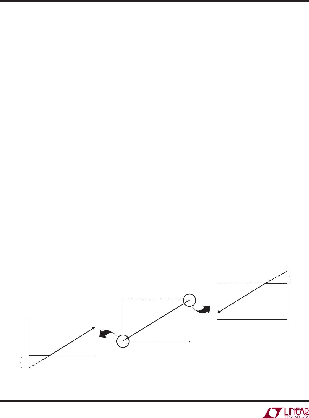
2600 F03
INPUT CODE
OUTPUT
VOLTAGE
NEGATIVE
OFFSET
0V
32,768
0
65,535
INPUT CODE
OUTPUT
VOLTAGE
V
REF
= V
CC
V
REF
= V
CC
INPUT CODE
OUTPUT
VOLTAGE
POSITIVE
FSE
Figure 3. Effects of Rail-to-Rail Operation On a DAC Transfer Curve. (a) Overall Transfer Function (b) Effect
of Negative Offset for Codes Near Zero Scale (c) Effect of Positive Full-Scale Error for Codes Near Full Scale
(b)
(a)
(c)
DC output impedance is equivalent to load regulation, and
may be derived from it by simply calculating a change in
units from LSB/mA to Ohms. The amplifi ers’ DC output
impedance is 0.025Ω when driving a load well away from
the rails.
When drawing a load current from either rail, the output
voltage headroom with respect to that rail is limited by
the 30Ω typical channel resistance of the output devices;
e.g., when sinking 1mA, the minimum output voltage =
30Ω • 1mA = 30mV. See the graph Headroom at Rails vs
Output Current in the Typical Performance Characteristics
section.
The amplifi ers are stable driving capacitive loads of up
to 1000pF.
Board Layout
The excellent load regulation and DC crosstalk performance
of these devices is achieved in part by keeping “signal”
and “power” grounds separate.
The PC board should have separate areas for the analog
and digital sections of the circuit. This keeps digital signals
away from sensitive analog signals and facilitates the use
of separate digital and analog ground planes which have
minimal capacitive and resistive interaction with each
other.
Digital and analog ground planes should be joined at only
one point, establishing a system star ground as close to
the device’s ground pin as possible. Ideally, the analog
ground plane should be located on the component side of
the board, and should be allowed to run under the part to
shield it from noise. Analog ground should be a continuous
and uninterrupted plane, except for necessary lead pads
and vias, with signal traces on another layer.
The GND pin functions as a return path for power sup-
ply currents in the device and should be connected to
analog ground. Resistance from the GND pin to system
star ground should be as low as possible. When a zero
scale DAC output voltage of zero is desired, the REFLO pin
(pin 2) should be connected to system star ground.
Rail-to-Rail Output Considerations
In any rail-to-rail voltage output device, the output is limited
to voltages within the supply range.
Since the analog outputs of the device cannot go below
ground, they may limit for the lowest codes as shown in
Figure 3b. Similarly, limiting can occur near full scale when
the REF pins are tied to V
CC
. If REF x = V
CC
and the DAC
full-scale error (FSE) is positive, the output for the highest
codes limits at V
CC
as shown in Figure 3c. No full-scale
limiting can occur if REF x is less than V
CC
– FSE.
Offset and linearity are defi ned and tested over the region
of the DAC transfer function where no output limiting
can occur.