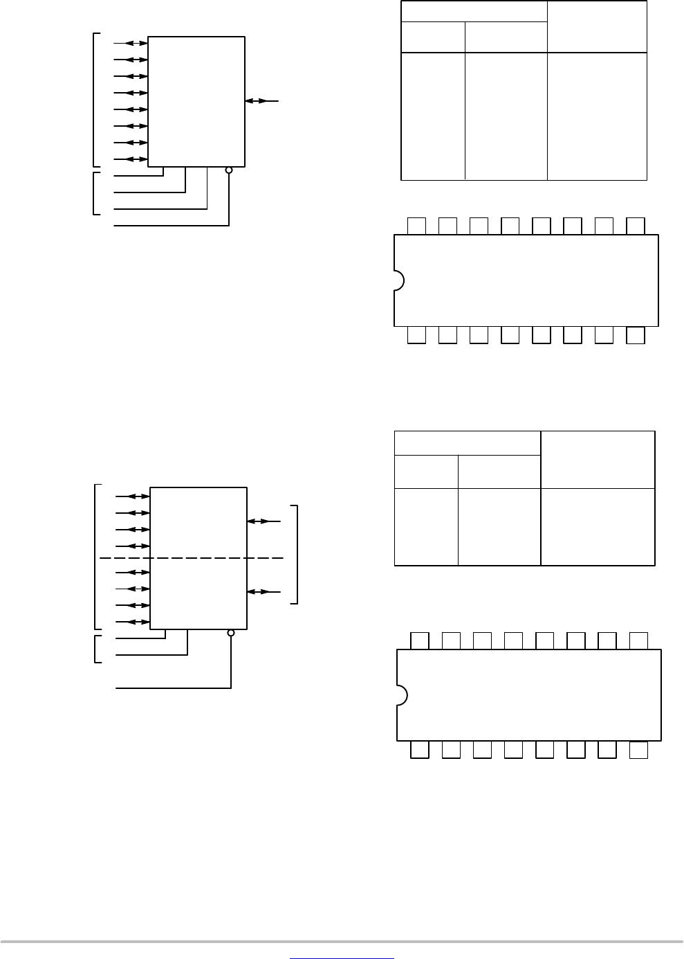
MC74HCT4851A, MC74HCT4852A
www.onsemi.com
3
MAXIMUM RATINGS
Symbol Parameter Value Unit
V
CC
Positive DC Supply Voltage (Referenced to GND) –0.5 to + 7.0 V
V
in
DC Input Voltage (Any Pin) (Referenced to GND) –0.5 to V
CC
+ 0.5 V
I DC Current, Into or Out of Any Pin $25 mA
P
D
Power Dissipation in Still Air, SOIC Package†
TSSOP Package†
500
450
mW
T
stg
Storage Temperature Range –65 to + 150 °C
T
L
Lead Temperature, 1 mm from Case for 10 Seconds
SOIC or TSSOP Package
260
°C
Stresses exceeding those listed in the Maximum Ratings table may damage the device. If any of
these limits are exceeded, device functionality should not be assumed, damage may occur and
reliability may be affected.
RECOMMENDED OPERATING CONDITIONS
Symbol Parameter Min Max Unit
V
CC
Positive DC Supply Voltage (Referenced to GND) 4.5 5.5 V
V
in
DC Input Voltage (Any Pin) (Referenced to GND) GND V
CC
V
V
IO
* Static or Dynamic Voltage Across Switch 0.0 1.2 V
T
A
Operating Temperature Range, All Package Types – 55 + 125 °C
t
r
, t
f
Input Rise/Fall Time V
CC
= 2.0 V
(Channel Select or Enable Inputs) V
CC
= 4.5 V
V
CC
= 6.0 V
0
0
0
1000
500
400
ns
Functional operation above the stresses listed in the Recommended Operating Ranges is not
implied. Extended exposure to stresses beyond the Recommended Operating Ranges limits may
affect device reliability.
*For voltage drops across switch greater than 1.2 V (switch on), excessive V
CC
current may be
drawn; i.e., the current out of the switch may contain both V
CC
and switch input components. The
reliability of the device will be unaffected unless the Maximum Ratings are exceeded.
DC CHARACTERISTICS — Digital Section (Voltages Referenced to GND) V
EE
= GND, Except Where Noted
Symbo
Parameter Condition
V
CC
V
Guaranteed Limit
Unit
−55 to 25°C ≤85°C ≤125°C
V
IH
Minimum High−Level Input Voltage,
Channel−Select or Enable Inputs
R
on
= Per Spec 4.5
to
5.5
2.0 2.0 2.0 V
V
IL
Maximum Low−Level Input Voltage,
Channel−Select or Enable Inputs
R
on
= Per Spec 4.5
to
5.5
0.8 0.8 0.8 V
I
in
Maximum Input Leakage Current on Digital Pins
(Enable/A/B/C)
V
in
= V
CC
or GND 5.5 ± 0.1 ± 1.0 ± 1.0
mA
I
CC
Maximum Quiescent Supply Current
(per Package)
V
in(digital)
= V
CC
or GND
V
in(analog)
= GND
5.5 2.0 20 40
mA
This device contains protection
circuitry to guard against damage
due to high static voltages or electric
fields. However, precautions must
be taken to avoid applications of any
voltage higher than maximum rated
voltages to this high−impedance cir-
cuit. For proper operation, V
in
and
V
out
should be constrained to the
range GND v (V
in
or V
out
) v V
CC
.
Unused inputs must always be
tied to an appropriate logic voltage
level (e.g., either GND or V
CC
).
Unused outputs must be left open.