ZL40214 Data Sheet
13
Microsemi Corporation
3.3 Device Additive Jitter
The ZL40214 clock fanout buffer is not intended to filter clock jitter. The jitter performance of this type of device is
characterized by its additive jitter. Additive jitter is the jitter the device would add to a hypothetical jitter-free clock as
it passes through the device. The additive jitter of the ZL40214 is random and as such it is not correlated to the jitter
of the input clock signal.
The square of the resultant random RMS jitter at the output
of the ZL40214 is equal to the sum of the squares of the
various random RMS jitter sources including: input clock jitter; additive jitter of the buffer; and additive jitter due to
power supply noise. There may be additional deterministic jitter sources, but they are not shown in Figure 17.
+
J
in
2
J
add
2
J
ps
2
J
in
= Random input clock jitter (RMS)
J
add
= Additive jitter due to the device (RMS)
J
ps
= Additive jitter due to power supply noise (RMS)
J
out
= Resultant random output clock jitter (RMS)
+
J
out
2
= J
in
2
+J
add
2
+J
ps
2
Figure 17 - Additive Jitter
ZL40214 Data Sheet
14
Microsemi Corporation
3.4 Power Supply
This device operates with either a 2.5V supply or 3.3V supply.
3.4.1 Sensitivity to power supply noise
Power supply noise from sources such as switching power supplies and high-power digital components such as
FPGAs can induce additive jitter on clock buffer outputs. The ZL40214 is equipped with a low drop out (LDO) power
regulator and on-chip bulk capacitors to minimize additive jitter due to power supply noise. The LDO regulator on
the ZL40214 allows this device to have superior performance even in the presence of external noise sources. The
on-chip measures in combination with the simple recommended power supply filtering and PCB layout minimize the
additive jitter from power supply noise.
The performance of these clock buffers in the presence o
f power supply noise is detailed in ZLAN-403, “Power
Supply Rejection in Clock Buffers” which is available from Applications Engineering.
3.4.2 Power supply filtering
For optimal jitter performance, the device should be isolated from the power planes connected to its power supply
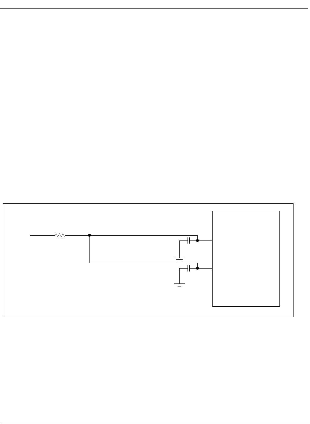
pins as shown in Figure 18.
10 µF capacitors should be size 0603 or size 080
5 X5R or X7R ceramic, 6.3 V minimum rating
0.1 µF capacitors should be
size 0402 X5R ceramic, 6.3 V minimum rating
Capacitors should be placed next to the
connected device power pins
a 0.3 ohm resistor is recommended for the filter shown in Figure 18
Figure 18 - Decoupling Connections for Power Pins
VDD
0.3 Ohms
0.1 µF
10 µF
ZL40214
8
13
3.4.3 PCB layout considerations
The power nets in Figure 18 can be implemented either as a plane island or routed power topology without
changing the overall jitter p
erformance of the device.
Absolute Maximum Ratings*
Parameter Sym. Min. Max. Units
1 Supply voltage V
DD_R
-0.5 4.6 V
2 Voltage on any digital pin V
PIN
-0.5 V
DD
V
3 Soldering temperature T 260 °C
4 Storage temperature T
ST
-55 125 °C
5 Junction temperature T
j
125 °C
6 Voltage on input pin V
input
V
DD
V
7 Input capacitance each pin C
p
500 fF
ZL40214 Data Sheet
15
Microsemi Corporation
4.0 AC and DC Electrical Characteristics
* Exceeding these values may cause permanent damage. Functional operation under these conditions is not implied.
* Voltages are with respect to ground (GND) unless otherwise stated
Recommended Operating Conditions*
Characteristics Sym. Min. Typ. Max. Units
1 Supply voltage 2.5 V mode V
DD25
2.375 2.5 2.625 V
2 Supply voltage 3.3 V mode V
DD33
3.135 3.3 3.465 V
3 Operating temperature T
A
-40 25 85 °C
* Voltages are with respect to ground (GND) unless otherwise stated
DC Electrical Characteristics - Current Consumption
Characteristics Sym. Min. Typ. Max. Units Notes
1 Supply current LVDS drivers -
loa
ded (all outputs are active)
I
dd_load
61 mA
DC Electrical Characteristics - Inputs and outputs - for 2.5/3.3 V supply
Characteristics Sym. Min. Typ. Max. Units Notes
1 LVDS Differential input common
m
ode voltage
V
ICM
1.1 1.6 V for 2.5 V
2 LVDS Differential input common
m
ode voltage
V
ICM
1.1 2.0 V for 3.3 V
3 LVDS Differential input voltage V
ID
0.25 1 V
4 LVDS output differential voltage* V
OD
0.25 0.30 0.40 V
5 LVDS output common mode voltage V
CM
1.1 1.25 1.375 V
* The VOD parameter was measured from 125 to 750 MHz.

ZL40214LDF1

Mfr. #:
Manufacturer:
Microchip / Microsemi
Description:
Clock Buffer 1:4 LVDS Fanout Buffer w/Ext. Term.
Lifecycle:
New from this manufacturer.
Delivery:
DHL FedEx Ups TNT EMS
Payment:
T/T Paypal Visa MoneyGram Western Union

Products related to this Datasheet