NJM2903/2403
-1-
Ver.2007-05-09
SINGLE-SUPPLY DUAL COMPARATOR
■ GENERAL DESCRIPTION ■ PACKAGE OUTLINE
The NJM2903/2403 consist of two independent precision voltage
comparators with an offset voltage specification as low as 5.0mV max for two
comparators, which were designed specifically to operate from a single
power supply over a wide range of voltages. Operation from split power
supplies is also possible and the low power supply current drain is
independent of the magnitude of the power supply voltage. The
NJM2903/2403 has a unique characteristic: the input common-mode voltage
range includes ground, even though operated from a single power supply
voltage. Application areas include limit comparators, simple analog-to-digital
converters; pulse, square-wave and time delay generators; wide range V
CO
;
MOS clock timers; multivibrators and high voltage digital logic gates. The
NJM2903/2403 were designed to directly interface with TTL and MOS.When
operated from both plus and minus power supplies, the NJM2903/2403 will
directly interface with MOS logic where their low power drain is a distinct
advantage over standard comparators.
■ FEATURES
● Operating Voltage ( +2V~+36V )
● Single Supply Operation
● Open Collector Output
● High Output Sink Current ( 15mA @ 2403 )
● Package Outline DIP8, DMP8, SIP8, SSOP8,
EMP8 (NJM2903 only), TVSP8 (NJM2903 only)
● Bipolar Technology
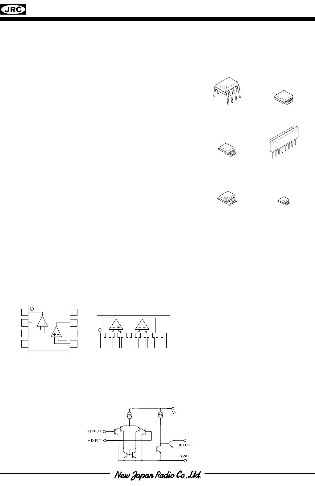
■ PIN CONFIGURATION
■ EQUIVALENT CIRCUIT ( 1/2 Shown )
8
7
6
5
1
2
3
4
A
B
( Top View )
A B
12345678
PIN FUNCTION
1. A OUTPUT
2. A –INPUT
3. A +INPUT
4. GND
5. B +INPUT
6. B –INPUT
7. B OUTPUT
8. V
+
NJM2903D/2403D
NJM2903M/2403M
NJM2903V/2403V
NJM2903E
NJM2903RB1
NJM2903L/2403L
NJM2903D/2403D NJM2903M/2403M
NJM2903L/2403LNJM2903V/2403V
NJM2903RB1 NJM2903E

