BUL381D
HIGH VOLTAGE FAST-SWITCHING
NPN POWER TRANSISTOR
■ STMicroelectronics PREFERRED
SALESTYPE
■ HIGH VOLTAGE CAPABILITY
■ LOW SPREAD OF DYNAMIC PARAMETERS
■ MINIMUM LOT-TO-LOT SPREAD FOR
RELIABLE OPERATION
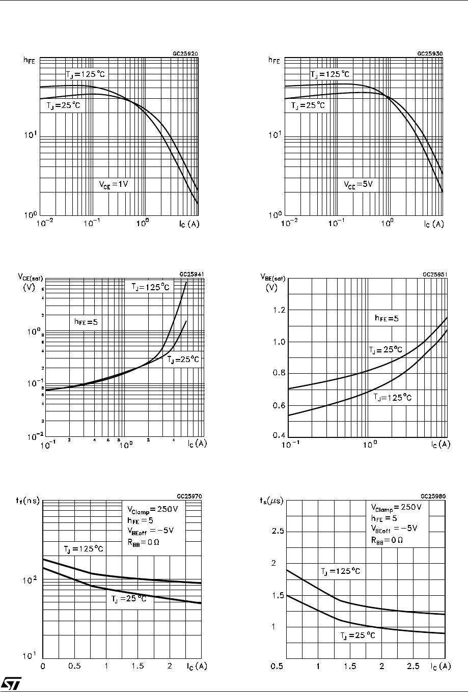
■ VERY HIGH SWITCHING SPEED
■ LARGE RBSOA
■ INTEGRATED ANTIPARALLEL
COLLECTOR-EMITTER DIODE
APPLICATIONS
■ ELECTRONIC TRANSFORMERS FOR
HALOGEN LAMPS
■ ELECTRONIC BALLASTS FOR
FLUORESCENT LIGHTING
■ SWITCH MODE POWER SUPPLIES
DESCRIPTION
The BUL381D is manufactured using high
voltage Multi Epitaxial Planar technology for high
switching speeds and high voltage capability.
The BUL series is designed for use in lighting
applications and low cost switch-mode power
supplies.
®
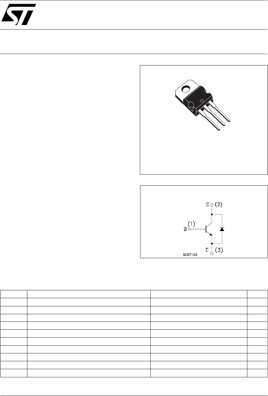
INTERNAL SCHEMATIC DIAGRAM
July 2003
ABSOLUTE MAXIMUM RATINGS
Symbol Parameter Value Unit
V
CES
Collector-Emitter Voltage (V
BE
= 0) 800 V
V
CEO
Collector-Emitter Voltage (I
B
= 0) 400 V
V
EBO
Emitter-Base Voltage (I
C
= 0) 9 V
I
C
Collector Current 5 A
I
CM
Collector Peak Current (t
p
< 5 ms) 8 A
I
B
Base Current 2 A
I
BM
Base Peak Current (t
p
< 5 ms) 4 A
P
tot
Total Dissipation at T
c
= 25
o
C70W
T
stg
Storage Temperature -65 to 150
o
C
T
j
Max. Operating Junction Temperature 150
o
C
1
2
3
TO-220
1/6