LM2931, NCV2931 Series
http://onsemi.com
11
0
50
100
150
200
250
300
0.0
0.6
1.0
1.2
1.4
1.8
010203025155.0
L, LENGTH OF COPPER (mm)
P
D(max)
for T
A
= 50°C
R
q
JA
, THERMAL RESISTANCE,
JUNCTION−TO−AIR (°CW)
P
D
, MAXIMUM POWER DISSIPATION (W)
R
q
JA
L
L
2.0 oz. Copper
0.4
1.6
0.2
0.8
30
40
50
60
70
80
1.0
1.5
2.0
2.5
3.0
3.5
010203025155.0
L, LENGTH OF COPPER (mm)
P
D(max)
for T
A
= 50°C
Minimum
Size Pad
2.0 oz. Copper
L
L
Free Air
Mounted
Vertically
P
D
, MAXIMUM POWER DISSIPATION (W)
R
q
JA
R , THERMAL RESISTANCE
JAθ
JUNCTION-TO-AIR ( C/W)°
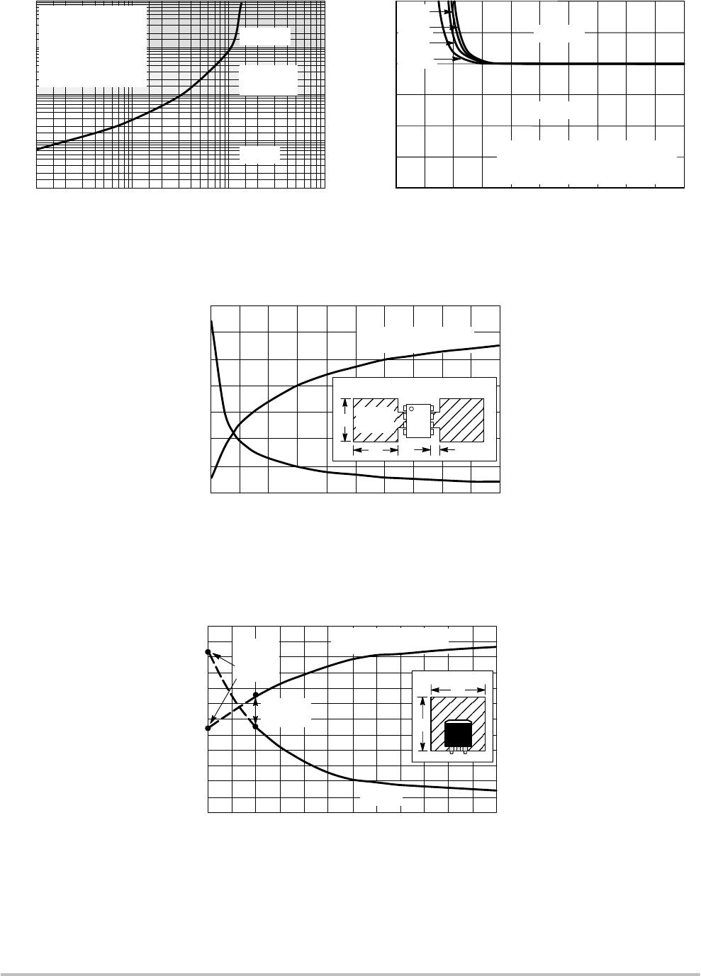
Figure 26. 3−Pin and 5−Pin D
2
PAK
Thermal Resistance and Maximum Power
Dissipation versus P.C.B. Copper Length
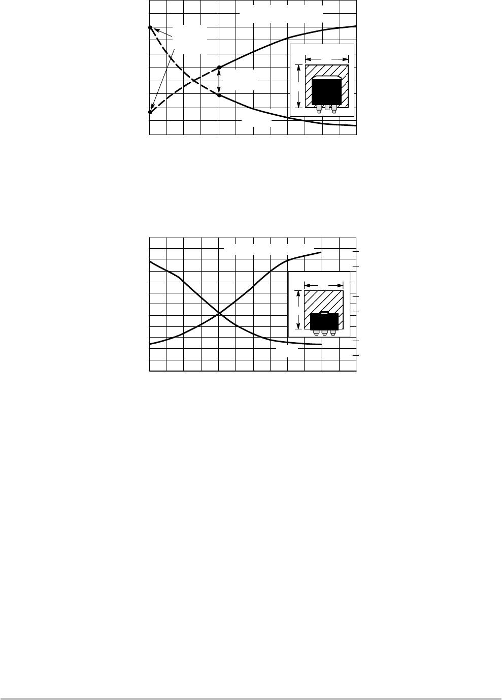
Figure 27. SOT−223 Thermal Resistance and Maximum
Power Dissipation vs. P.C.B. Copper Length
DEFINITIONS
Dropout Voltage − The input/output voltage differential
at which the regulator output no longer maintains regulation
against further reductions in input voltage. Measured when
the output decreases 100 mV from nominal value at 14 V
input, dropout voltage is affected by junction temperature
and load current.
Line Regulation − The change in output voltage for a
change in the input voltage. The measurement is made under
conditions of low dissipation or by using pulse techniques
such that the average chip temperature is not significantly
affected.
Load Regulation − The change in output voltage for a
change in load current at constant chip temperature.
Maximum Power Dissipation − The maximum total
device dissipation for which the regulator will operate
within specifications.
Bias Current − That part of the input current that is not
delivered to the load.
Output Noise Voltage − The rms AC voltage at the
output, with constant load and no input ripple, measured
over a specified frequency range.
Long−Term Stability − Output voltage stability under
accelerated life test conditions with the maximum rated
voltage listed in the devices electrical characteristics and
maximum power dissipation.