IDT8T49N008ANLGI REVISION A FEBRUARY 13, 2014 24 ©2014 Integrated Device Technology, Inc.
IDT8T49N008I Data Sheet PROGRAMMABLE FEMTOCLOCK
®
NG LVPECL/LVDS CLOCK GENERATOR WITH 8-OUTPUTS
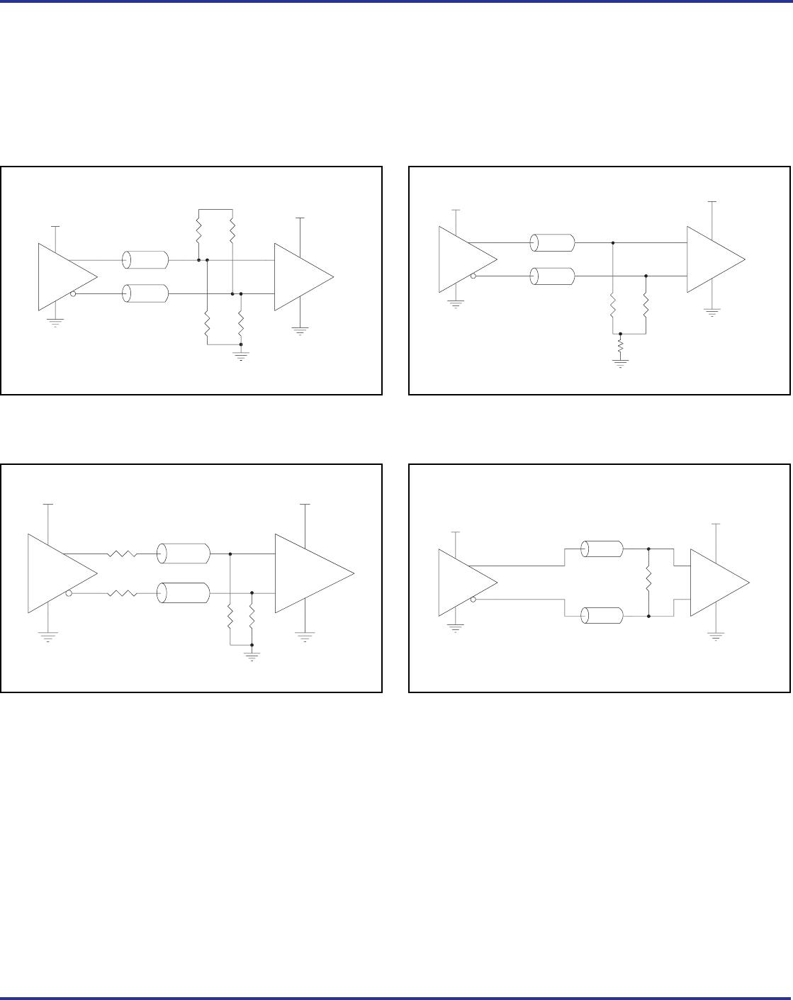
LVDS Driver Termination
For a general LVDS interface, the recommended value for the
termination impedance (Z
T
) is between 90 and 132. The actual
value should be selected to match the differential impedance (Z
0
) of
your transmission line. A typical point-to-point LVDS design uses a
100 parallel resistor at the receiver and a 100 differential
transmission-line environment. In order to avoid any
transmission-line reflection issues, the components should be
surface mounted and must be placed as close to the receiver as
possible. IDT offers a full line of LVDS compliant devices with two
types of output structures: current source and voltage source. The
standard termination schematic as shown in Figure 5A can be used
with either type of output structure. Figure 5B, which can also be
used with both output types, is an optional termination with center tap
capacitance to help filter common mode noise. The capacitor value
should be approximately 50pF. If using a non-standard termination, it
is recommended to contact IDT and confirm if the output structure is
current source or voltage source type. In addition, since these
outputs are LVDS compatible, the input receiver’s amplitude and
common-mode input range should be verified for compatibility with
the output.
Termination for 3.3V LVPECL Outputs
The clock layout topology shown below is a typical termination for
LVPECL outputs. The two different layouts mentioned are
recommended only as guidelines.
The differential outputs are low impedance follower outputs that
generate ECL/LVPECL compatible outputs. Therefore, terminating
resistors (DC current path to ground) or current sources must be
used for functionality. These outputs are designed to drive 50
transmission lines. Matched impedance techniques should be used
to maximize operating frequency and minimize signal distortion.
Figures 6A and 6B show two different layouts which are
recommended only as guidelines. Other suitable clock layouts may
exist and it would be recommended that the board designers
simulate to guarantee compatibility across all printed circuit and clock
component process variations.
Figure 6A. 3.3V LVPECL Output Termination Figure 6B. 3.3V LVPECL Output Termination
LVDS
Driver
LVDS
Driver
LVDS
Receiver
LVDS
Receiver
Z
T
C
Z
O
Z
T
Z
O
Z
T
Z
T
2
Z
T
2
Figure 5A. Standard Termination
Figure 5B. Optional Termination
R1
84
R2
84
3.3V
R3
125
R4
125
Z
o
= 50
Z
o
= 50
LVPECL Input
3.3V
3.3V
+
_