IDT8T49N008ANLGI REVISION A FEBRUARY 13, 2014 6 ©2014 Integrated Device Technology, Inc.
IDT8T49N008I Data Sheet PROGRAMMABLE FEMTOCLOCK
®
NG LVPECL/LVDS CLOCK GENERATOR WITH 8-OUTPUTS
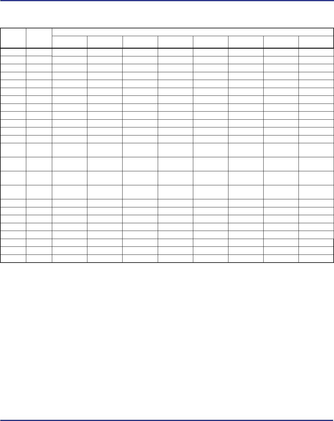
Table 3C. I
2
C Function Descriptions
Bits Name Function
Pn[1:0]
Input Clock Divider Register n
(n = 0...3)
Sets the PLL input clock divider. The divider value has the range of 1, 2,
4 and 5. See Table 3F. Pn[1:0] bits are programmed with values to
support default configuration settings for FSEL[1:0].
PSn(1:0)
Input Prescaler Register n
(n = 0...3)
Sets the PLL input clock prescaler value. Valid prescaler values are x0.5,
x1 or x2. See Table 3F. Set prescaler to x2 for optimum phase noise
performance. PSn[1:0] bits are programmed with values to support
default configuration settings for FSEL[1:0].
Mn[8:1]
Integer Feedback Divider
Register n
(n = 0...3)
Sets the integer feedback divider value. Based on the FemtoClock NG
VCO range, the applicable feedback dividers settings are 16 thru 250.
Please note the register value presents bits [8:1] of Mn, the LSB of Mn is
not in the register. Mn[8:1] bits are programmed with values to support
default configuration settings for FSEL[1:0].
Nn[6:0]
Output Divider Register n
(n = 0...3)
Sets the output divider. The output divider value can range from 2, 3, 4,
5, 6 and 8, 10, 12 to 126 (step: 2). See Table 3G for the output divider
coding. Nn[6:0] bits are programmed with values to support default
configuration settings for FSEL[1:0].
CPn[1:0]
PLL Bandwidth Register n
(n = 0...3)
Sets the FemtoClock NG PLL bandwidth by controlling the charge pump
current. See Table 3H. CPn[1:0] bits are programmed with values to
support default configuration settings for FSEL[1:0].
BYPASSn
PLL Bypass Register n
(n = 0...3)
Bypasses PLL. Output of the prescaler is routed through the output
divider N to the output fanout buffer. Programming a 1 to this bit
bypasses the PLL. Programming a 0 to this bit routes the output of the
prescaler through the PLL. BYPASSn bits are programmed with values
to support default configuration settings for FSEL[1:0].
OEn[Q0]
OEn[Q1]
OEn[Q2]
OEn[Q3]
OEn[Q4]
OEn[Q5]
OEn[Q6]
OEn[Q7]
Output Enable Register n
(n = 0...3)
Sets the outputs to Active or High Impedance. Programming a 0 to this
bit sets the outputs to High Impedance. Programming a 1 sets the
outputs to active status. OEn[Q0], OEn[Q1], OEn[Q2], OEn[Q3],
OEn[Q4], OEn[Q5], OEn[Q6], OEn[Q7] bits are programmed with values
to support default configuration settings for FSEL[1:0].
LVDS_SELn[Q0]
LVDS_SELn[Q1]
LVDS_SELn[Q2]
LVDS_SELn[Q3]
LVDS_SELn[Q4]
LVDS_SELn[Q5]
LVDS_SELn[Q6]
LVDS_SELn[Q7]
Output Style Register n
(n = 0...3)
Sets the differential output style to either LVDS or LVPECL interface
levels. Programming a 1 to this bit sets the output styles to LVDS levels.
Programming a 0 to this bit sets the output styles to LVPECL levels.
LVDS_SELn[Q0], LVDS_SELn[Q1], LVDS_SELn[Q2], LVDS_SELn[Q3]
LVDS_SELn[Q4], LVDS_SELn[Q5], LVDS_SELn[Q6], LVDS_SELn[Q7]
bits are programmed with values to support default configuration settings
for FSEL[1:0].