IXTY1R6N50D2 IXTA1R6N50D2
IXTP1R6N50D2
IXYS Reserves the Right to Change Limits, Test Conditions, and Dimensions.
Symbol Test Conditions Characteristic Values
(T
J
= 25°C, Unless Otherwise Specified) Min. Typ. Max.
g
fs
V
DS
= 30V, I
D
= 0.8A, Note 1 1.00 1.75 S
C
iss
645 pF
C
oss
V
GS
= -10V, V
DS
= 25V, f = 1MHz 65 pF
C
rss
16.5 pF
t
d(on)
25 ns
t
r
70 ns
t
d(off)
35 ns
t
f
41 ns
Q
g(on)
23.7 nC
Q
gs
V
GS
= 5V, V
DS
= 250V, I
D
= 0.8A 2.2 nC
Q
gd
13.8 nC
R
thJC
1.25 °C/W
R
thCS
TO-220 0.50 °C/W
Safe-Operating-Area Specification
Characteristic Values
Symbol Test Conditions Min. Typ. Max.
SOA V
DS
= 400V, I
D
= 0.15A, T
C
= 75°C, Tp = 5s 60 W
Source-Drain Diode
Symbol Test Conditions Characteristic Values
(T
J
= 25°C, Unless Otherwise Specified) Min. Typ. Max.
V
SD
I
F
= 1.6A, V
GS
= -10V, Note 1 0.8 1.3 V
t
rr
400 ns
I
RM
9.16 A
Q
RM
1.83 μC
IXYS MOSFETs and IGBTs are covered 4,835,592 4,931,844 5,049,961 5,237,481 6,162,665 6,404,065 B1 6,683,344 6,727,585 7,005,734 B2 7,157,338B2
by one or more of the following U.S. patents: 4,850,072 5,017,508 5,063,307 5,381,025 6,259,123 B1 6,534,343 6,710,405 B2 6,759,692 7,063,975 B2
4,881,106 5,034,796 5,187,117 5,486,715 6,306,728 B1 6,583,505 6,710,463 6,771,478 B2 7,071,537
Note 1. Pulse test, t ≤ 300μs, duty cycle, d ≤ 2%.
Resistive Switching Times
V
GS
= ±5V, V
DS
= 250V, I
D
= 0.8A
R
G
= 5Ω (External)
I
F
= 1.6A, -di/dt = 100A/μs
V
R
= 100V, V
GS
= -10V
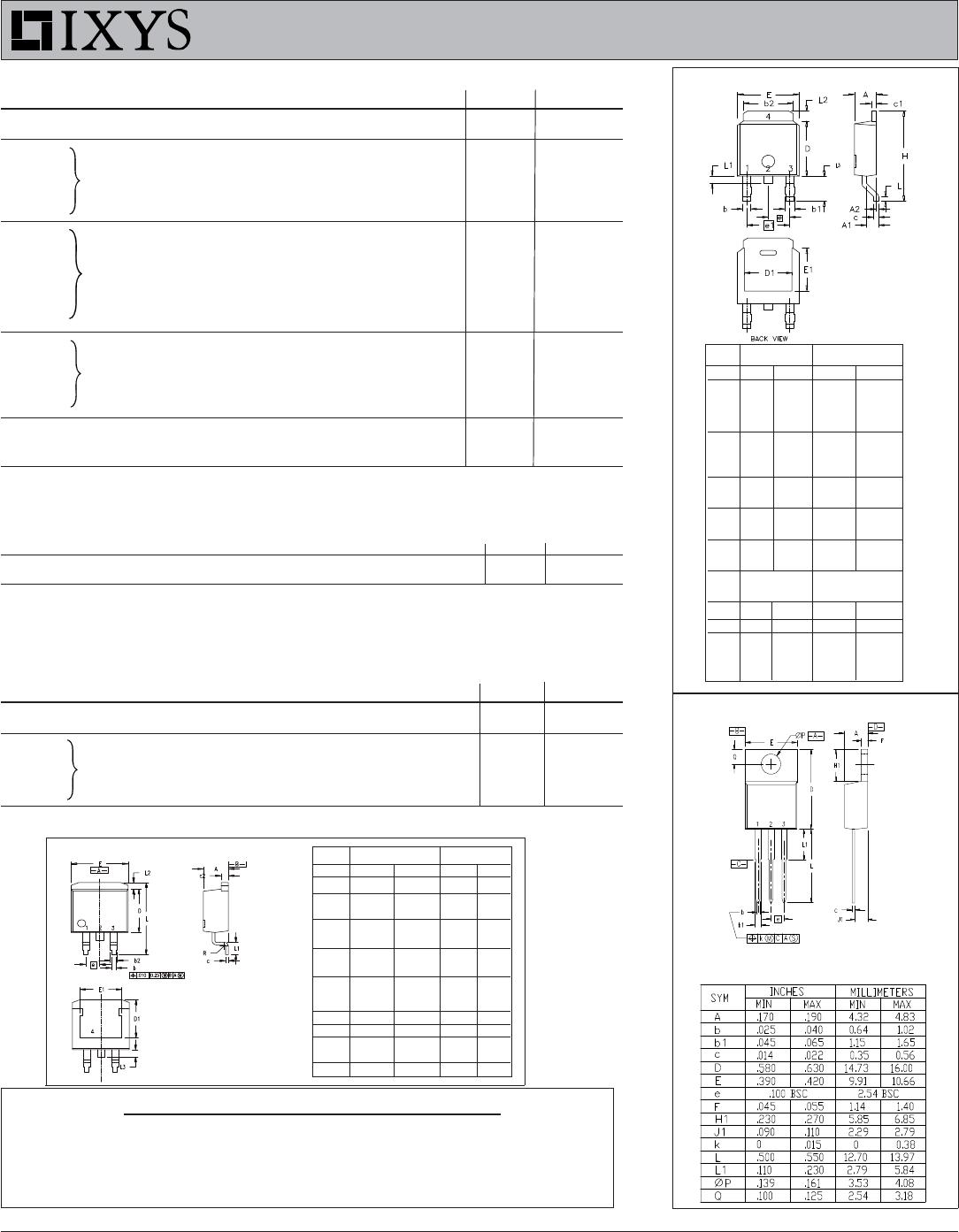
Pins: 1 - Gate 2 - Drain
3 - Source 4 - Drain
TO-220 (IXTP) Outline
TO-263 (IXTA) Outline
1. Gate
2. Drain
3. Source
4. Drain
Dim. Millimeter Inches
Min. Max. Min. Max.
A 4.06 4.83 .160 .190
b 0.51 0.99 .020 .039
b2 1.14 1.40 .045 .055
c 0.40 0.74 .016 .029
c2 1.14 1.40 .045 .055
D 8.64 9.65 .340 .380
D1 8.00 8.89 .280 .320
E 9.65 10.41 .380 .405
E1 6.22 8.13 .270 .320
e 2.54 BSC .100 BSC
L 14.61 15.88 .575 .625
L1 2.29 2.79 .090 .110
L2 1.02 1.40 .040 .055
L3 1.27 1.78 .050 .070
PRELIMINARY TECHNICAL INFORMATION
The product presented herein is under development. The Technical Specifications offered are derived
from data gathered during objective characterizations of preliminary engineering lots; but also may yet
contain some information supplied during a pre-production design evaluation. IXYS reserves the right
to change limits, test conditions, and dimensions without notice.
TO-252 AA (IXTY) Outline
Dim. Millimeter Inches
Min. Max. Min. Max.
A 2.19 2.38 0.086 0.094
A1 0.89 1.14 0.035 0.045
A2 0 0.13 0 0.005
b 0.64 0.89 0.025 0.035
b1 0.76 1.14 0.030 0.045
b2 5.21 5.46 0.205 0.215
c 0.46 0.58 0.018 0.023
c1 0.46 0.58 0.018 0.023
D 5.97 6.22 0.235 0.245
D1 4.32 5.21 0.170 0.205
E 6.35 6.73 0.250 0.265
E1 4.32 5.21 0.170 0.205
e 2.28 BSC 0.090 BSC
e1 4.57 BSC 0.180 BSC
H 9.40 10.42 0.370 0.410
L 0.51 1.02 0.020 0.040
L1 0.64 1.02 0.025 0.040
L2 0.89 1.27 0.035 0.050
L3 2.54 2.92 0.100 0.115
1. Gate
2. Drain
3. Source
4. Drain
Bottom Side

