6N1135, 6N1136
www.vishay.com
Vishay Semiconductors
End of Life January-2018 - Alternative Device: 6N135, 6N136
Rev. 1.9, 13-Nov-12
1
Document Number: 83909
For technical questions, contact: optocoupleranswers@vishay.com
THIS DOCUMENT IS SUBJECT TO CHANGE WITHOUT NOTICE. THE PRODUCTS DESCRIBED HEREIN AND THIS DOCUMENT
ARE SUBJECT TO SPECIFIC DISCLAIMERS, SET FORTH AT www.vishay.com/doc?91000
High Speed Optocoupler, 1 MBd,
Photodiode with Transistor Output,
110 °C Rated
DESCRIPTION
The 6N1135 and 6N1136 are 110 °C rated optocouplers
with a GaAIAs infrared emitting diode, optically coupled with
an integrated photo detector which consists of a photo
diode and a high-speed transistor in a DIP-8 plastic
package.
Signals can be transmitted between two electrically
separated circuits up to frequencies of 2 MHz. The potential
difference between the circuits to be coupled should not
exceed the maximum permissible reference voltages.
FEATURES
• Operating temperature from -55 °C to +110 °C
• Isolation test voltages: 5300 V
RMS
• TTL compatible
• High bit rates: 1 MBd
•Bandwidth 2 MHz
• Open-collector output
• External base wiring possible
• Material categorization: for definitions of compliance
please see www.vishay.com/doc?99912
AGENCY APPROVALS
• UL1577 (pending)
• DIN EN 60747-5-5 (VDE 0884) (pending)
•cUL (pending)
• CQC (pending)
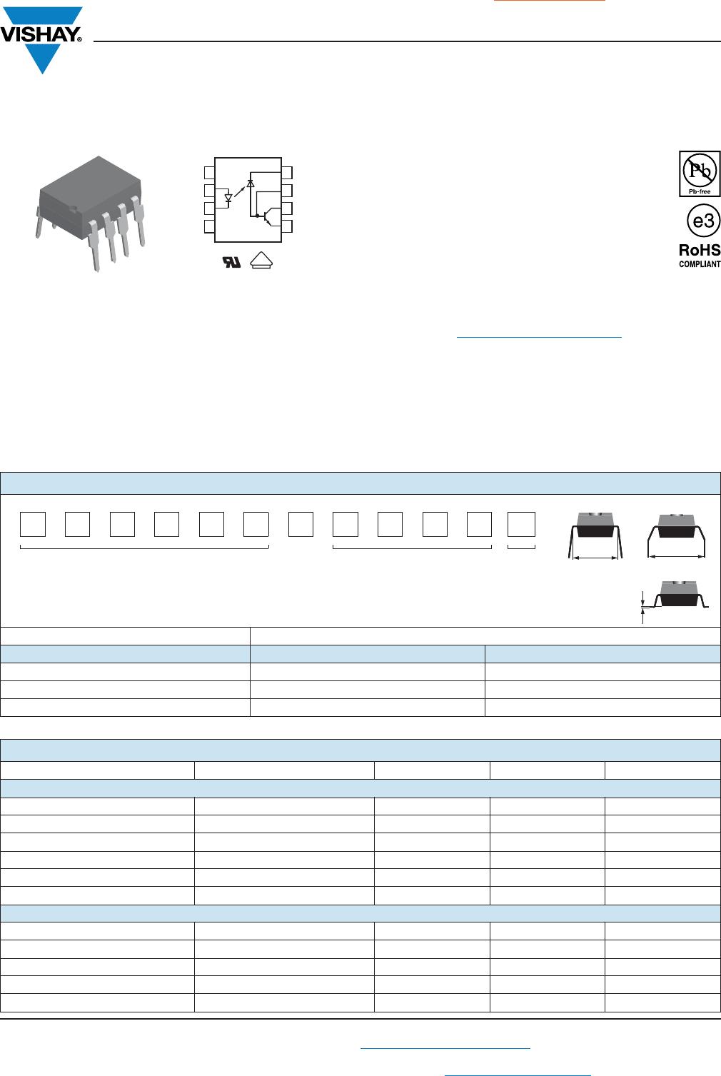
i179081_3
1
2
3
4
8
7
6
5
C (V
CC
)
NC
A
C
NC
B (V
B
)
C (V
O
)
E (GND)
V
DE
ORDERING INFORMATION
6N113#-X00#T
PART NUMBER PACKAGE OPTION TAPE
AND
REEL
AGENCY CERTIFIED/PACKAGE CTR (%)
UL ≥ 7 ≥ 19
DIP-8 6N1135 6N1136
DIP-8, 400 mil, option 6 6N1135-X006 6N1136-X006
SMD-8, option 9 6N1135-X009T 6N1136-X009T
ABSOLUTE MAXIMUM RATINGS (T
amb
= 25 °C, unless otherwise specified)
PARAMETER TEST CONDITION SYMBOL VALUE UNIT
INPUT
Reverse voltage V
R
5V
Forward current I
F
25 mA
Peak forward current t = 1 ms, duty cycle 50 % I
FM
50 mA
Maximum surge forward current t ≤ 1 μs, 300 pulses/s I
FSM
1A
Thermal resistance R
th
700 K/W
Power dissipation T
amb
= 70 °C P
diss
45 mW
OUTPUT
Supply voltage V
CC
-0.5 to 15 V
Output voltage V
O
-0.5 to 15 V
Emitter base voltage V
EBO
5V
Output current I
O
8mA
Maximum Output current 16 mA
> 0.1 mm
10.16 mm
7.62 mm
DIP-8
Option 6
Option 9