LTC1863/LTC1867
9
18637fc
For more information www.linear.com/LTC1863
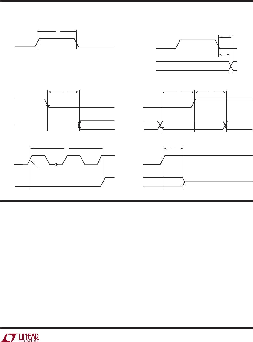
TIMING DIAGRAMS
t
5
(SDI Setup Time Before SCK↑),
t
6
(SDI Hold Time After SCK↑)
50%
50%
t
3
0.4V
t
7
(SLEEP Mode Wake-Up Time)
t
7
SCK
CS/CONV
t
8
(BUS Relinquish Time)
t
8
CS/CONV
SDO
2.4V
t
4
(SDO Valid After CONV↓)
t
4
CS/CONV
SDO
2.4V
0.4V
0.4V
t
6
2.4V
0.4V
t
5
SCK
SDI
2.4V
2.4V
0.4V
2.4V
0.4V
SDO
1867 TD
SLEEP BIT (SLP = 0)
READ-IN
10%
90%
Hi-Z
Hi-Z
t
1
(For Short Pulse Mode)
t
2
(SDO Valid Before SCK↑),
t
3
(SDO Valid Hold Time After SCK↓)
t
1
CS/CONV
t
2
SCK
50%
50%
Overview
The LTC1863/LTC1867 are complete, low power multi-
plexed ADCs. They consist of a 12-/16-bit, 200ksps capaci-
tive successive approximation A/D converter, a precision
internal reference, a configurable 8-channel analog input
multiplexer (MUX) and a serial port for data transfer.
Conversions are started by a rising edge on the CS/CONV
input. Once a conversion cycle has begun, it cannot be
restarted. Between conversions, the
ADCs receive an input
word for channel selection and output the conversion
result, and the analog input is acquired in preparation for
the next conversion. In the acquire phase, a minimum time
of 1.5µs will provide enough time for the sample-and-hold
capacitors to acquire the analog signal.
During the conversion, the internal differential 16-bit
capacitive DAC output is sequenced by the SAR from
the most
significant bit (MSB) to the least significant bit
(LSB). The input is successively compared with the binary
weighted charges supplied by the differential capacitive
DAC. Bit decisions are made by a low-power, differential
comparator. At the end of a conversion, the DAC output
balances the analog input. The SAR contents (a 12-/16-bit
data word) that represent the analog input are loaded into
the 12-/16-bit output
latches.
APPLICATIONS INFORMATION