AD8397
Rev. A | Page 11 of 16
APPLICATIONS INFORMATION
The AD8397 is a voltage feedback operational amplifier that
features an H-bridge input stage and common-emitter, rail-to-rail
output stage. The AD8397 can operate from a wide supply range,
±1.5 V to ±12 V. When driving light loads, the rail-to-rail output is
capable of swinging to within 0.2 V of either rail. The output can
also deliver high linear output current when driving heavy loads,
up to 310 mA into 32 Ω while maintaining −80 dBc SFDR. The
AD8397 is fabricated on Analog Devices proprietary XFCB-HV.
POWER SUPPLY AND DECOUPLING
The AD8397 can be powered with a good quality, well-regulated,
low noise supply from ±1.5 V to ±12 V. Pay careful attention to
decoupling the power supply. Use high quality capacitors with
low equivalent series resistance (ESR), such as multilayer
ceramic capacitors (MLCCs), to minimize the supply voltage
ripple and power dissipation. Locate a 0.1 μF MLCC decoupling
capacitor(s) no more than 1/8 inch away from the power supply
pin(s). A large tantalum 10 μF to 47 μF capacitor is recommended
to provide good decoupling for lower frequency signals and to
supply current for fast, large signal changes at the AD8397 outputs.
LAYOUT CONSIDERATIONS
As with all high speed applications, pay careful attention to
printed circuit board (PCB) layout to prevent associated board
parasitics from becoming problematic. The PCB should have a
low impedance return path (or ground) to the supply. Removing
the ground plane from all layers in the immediate area of the
amplifier helps to reduce stray capacitances. The signal routing
should be short and direct in order to minimize the parasitic
inductance and capacitance associated with these traces. Locate
termination resistors and loads as close as possible to their
respective inputs and outputs. Keep input traces as far apart as
possible from the output traces to minimize coupling (crosstalk)
though the board.
When the AD8397 is configured as a differential driver, as in
some line driving applications, provide a symmetrical layout to
the extent possible in order to maximize balanced performance.
When running differential signals over a long distance, the traces
on the PCB should be close together or any differential wiring
should be twisted together to minimize the area of the inductive
loop that is formed. This reduces the radiated energy and makes
the circuit less susceptible to RF interference. Adherence to
stripline design techniques for long signal traces (greater than
approximately 1 inch) is recommended.
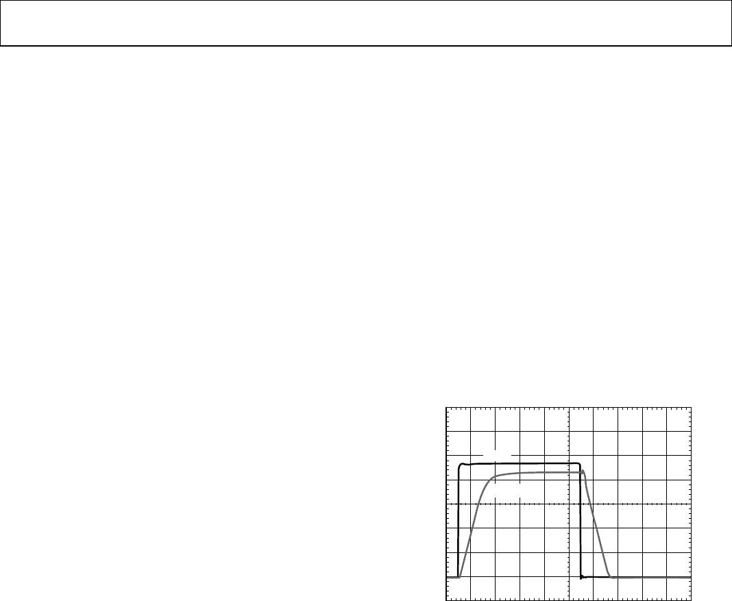
UNITY-GAIN OUTPUT SWING
When operating the AD8397 in a unity-gain configuration,
the output does not swing to the rails and is constrained by
the H-bridge input. This can be seen by comparing the output
overdrive recovery in Figure 7 and the input overdrive recovery in
Figure 22. To avoid overdriving the input and to realize the full
swing afforded by the rail-to-rail output stage, use the amplifier
in a gain of two or greater.
05069-028
INPUT
OUTPUT
7
–1
0
1
0 80 160 240 320 400
TIME (ns)
480 560 640 720 800
2
3
4
5
6
VOLTS
Figure 22. Unity-Gain Input Overdrive Recovery

