19
2271f
LTC2271
APPLICATIONS INFORMATION
The fi rst bit of the 16-bit input word is the R/W bit. The
next seven bits are the address of the register (A6:A0).
The fi nal eight bits are the register data (D7:D0).
If the R/W bit is low, the serial data (D7:D0) will be writ-
ten to the register set by the address bits (A6:A0). If the
R/W bit is high, data in the register set by the address bits
(A6:A0) will be read back on the SDO pin (see the Timing
Diagrams). During a read back command the register is
not updated and data on SDI is ignored.
The SDO pin is an open-drain output that pulls to ground
with a 200 impedance. If register data is read back
through SDO, an external 2k pull-up resistor is required.
If serial data is only written and read back is not needed,
Table 4. Serial Programming Mode Register Map (PAR/SER = GND)
REGISTER A0: RESET REGISTER (ADDRESS 00h)
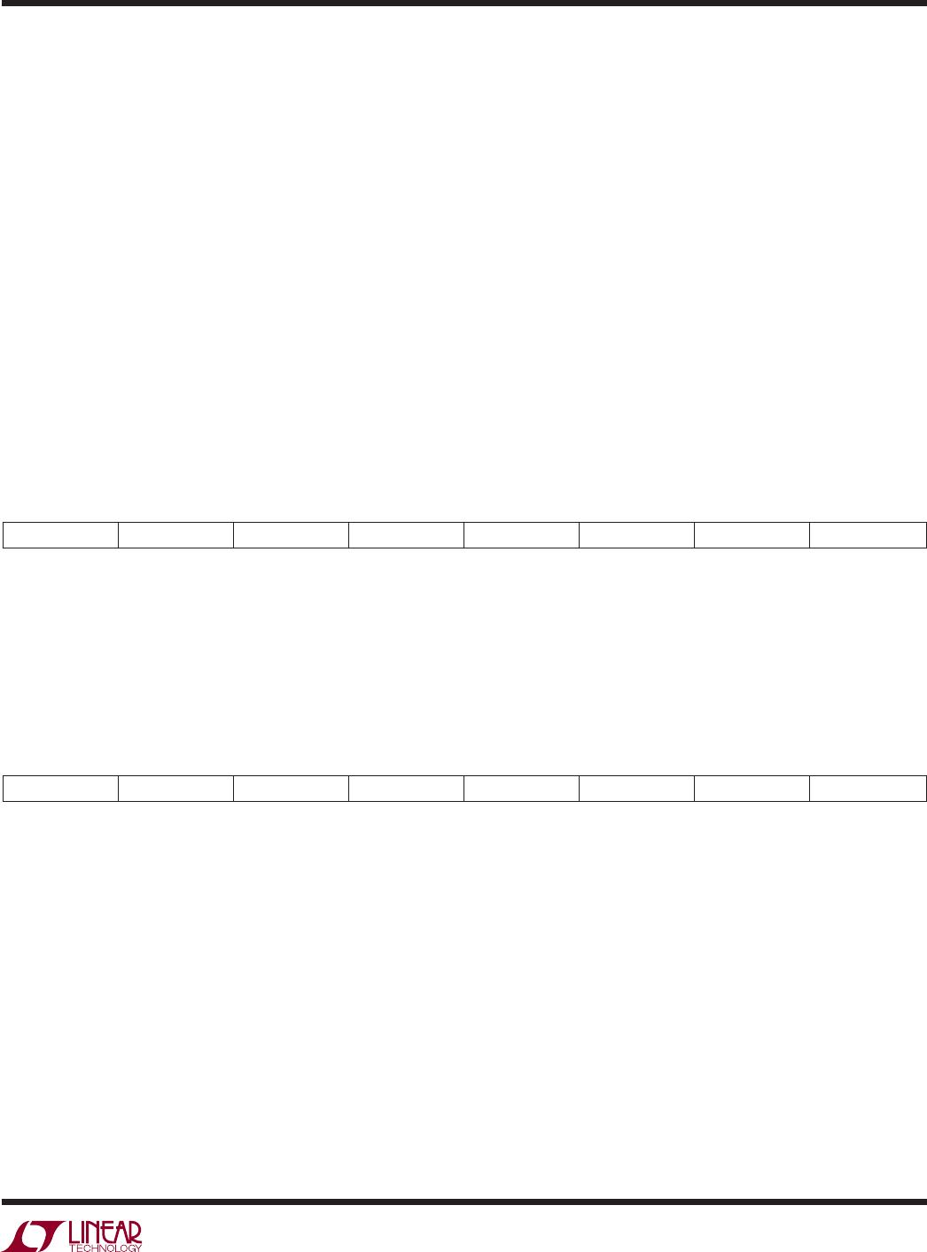
D7 D6 D5 D4 D3 D2 D1 D0
RESETXXXXXXX
Bit 7 RESET Software Reset Bit
0 = Not Used
1 = Software Reset. All Mode Control Registers are Reset to 00h. The ADC is Momentarily Placed in Sleep Mode.
This Bit is Automatically Set Back to Zero at the end of the SPI write command. The Reset register is write-only.
Data read back from the Reset register will be random.
Bits 6-0 Unused, Don’t Care Bits.
REGISTER A1: FORMAT AND POWER-DOWN REGISTER (ADDRESS 01h)
D7 D6 D5 D4 D3 D2 D1 D0
DCSOFF RAND TWOSCOMP SLEEP NAP_2 X X NAP_1
Bit 7 DCSOFF Clock Duty Cycle Stabilizer Bit
0 = Clock Duty Cycle Stabilizer On
1 = Clock Duty Cycle Stabilizer Off. This is not recommended.
Bit 6 RAND Data Output Randomizer Mode Control Bit
0 = Data Output Randomizer Mode Off
1 = Data Output Randomizer Mode On
Bit 5 TWOSCOMP Two’s Complement Mode Control Bit
0 = Offset Binary Data Format
1 = Two’s Complement Data Format
Bits 4, 3, 0 SLEEP:NAP_2:NAP_1 Sleep/Nap Mode Control Bits
000 = Normal Operation
0X1 = Channel 1 in Nap Mode
01X = Channel 2 in Nap Mode
1XX = Sleep Mode. Both Channels are Disabled.
Note: Any Combination of Channels Can Be Placed in Nap Mode
Bits 1, 2 Unused, Don’t Care Bits
then SDO can be left fl oating and no pull-up resistor is
needed.
Table 4 shows a map of the mode control registers.
Software Reset
If serial programming is used, the mode control registers
should be programmed as soon as possible after the power
supplies turn on and are stable. The fi rst serial command
must be a software reset which will reset all register data
bits to logic 0. To perform a software reset, bit D7 in the
reset register is written with a logic 1. After the reset SPI
write command is complete, bit D7 is automatically set
back to zero.
LTC2271
20
2271f
APPLICATIONS INFORMATION
REGISTER A2: OUTPUT MODE REGISTER (ADDRESS 02h)
D7 D6 D5 D4 D3 D2 D1 D0
ILVDS2 ILVDS1 ILVDS0 TERMON OUTOFF OUTTEST OUTMODE1 OUTMODE0
Bits 7-5 ILVDS2:ILVDS0 LVDS Output Current Bits
000 = 3.5mA LVDS Output Driver Current
001 = 4.0mA LVDS Output Driver Current
010 = 4.5mA LVDS Output Driver Current
011 = Not Used
100 = 3.0mA LVDS Output Driver Current
101 = 2.5mA LVDS Output Driver Current
110 = 2.1mA LVDS Output Driver Current
111 = 1.75mA LVDS Output Driver Current
Bit 4 TERMON LVDS Internal Termination Bit
0 = Internal Termination Off
1 = Internal Termination On. LVDS Output Driver Current is 2× the Current Set by ILVDS2:ILVDS0
Bit 3 OUTOFF Output Disable Bit
0 = Digital Outputs are Enabled
1 = Digital Outputs are Disabled
Bit 2 OUTTEST Digital Output Test Pattern Control Bit
0 = Digital Output Test Pattern Off
1 = Digital Output Test Pattern On
Bits 1-0 OUTMODE1:OUTMODE0 Digital Output Mode Control Bits
00 = 2-Lane Output Mode
01 = 4-Lane Output Mode
10 = 1-Lane Output Mode
11 = Not Used
REGISTER A3: TEST PATTERN MSB REGISTER (ADDRESS 03h)
D7 D6 D5 D4 D3 D2 D1 D0
TP15 TP14 TP13 TP12 TP11 TP10 TP9 TP8
Bits 7-0 TP15:TP8 Test Pattern Data Bits (MSB)
TP15:TP8 Set the Test Pattern for Data Bit 15 (MSB) Through Data Bit 8.
REGISTER A4: TEST PATTERN LSB REGISTER (ADDRESS 04h)
D7 D6 D5 D4 D3 D2 D1 D0
TP7 TP6 TP5 TP4 TP3 TP2 TP1 TP0
Bits 7-0 TP7:TP0 Test Pattern Data Bits (LSB)
TP7:TP0 Set the Test Pattern for Data Bit 7 Through Data Bit 0 (LSB).
21
2271f
LTC2271
APPLICATIONS INFORMATION
GROUNDING AND BYPASSING
The LTC2271 require a printed circuit board with a clean
unbroken ground plane. A multilayer board with an in-
ternal ground plane in the fi rst layer beneath the ADC is
recommended. Layout for the printed circuit board should
ensure that digital and analog signal lines are separated as
much as possible. In particular, care should be taken not
to run any digital track alongside an analog signal track
or underneath the ADC.
High quality ceramic bypass capacitors should be used at
the V
DD
, OV
DD
, V
CM
, V
REF
, REFH and REFL pins. Bypass
capacitors must be located as close to the pins as possible.
Size 0402 ceramic capacitors are recommended. The traces
connecting the pins and bypass capacitors must be kept
short and should be made as wide as possible.
Of particular importance is the capacitor between REFH
and REFL. This capacitor should be on the same side of
the circuit board as the A/D, and as close to the device
as possible.
The analog inputs, encode signals, and digital outputs
should not be routed next to each other. Ground fi ll and
grounded vias should be used as barriers to isolate these
signals from each other.
HEAT TRANSFER
Most of the heat generated by the LTC2271 is transferred
from the die through the bottom-side exposed pad and
package leads onto the printed circuit board. For good
electrical and thermal performance, the exposed pad must
be soldered to a large grounded pad on the PC board. This
pad should be connected to the internal ground planes by
an array of vias.
TYPICAL APPLICATIONS
LTC2271
V
CM1
GND
A
IN1
+
A
IN1
GND
REFH
REFL
REFH
REFL
PAR/SER
A
IN2
+
A
IN2
GND
V
CM2
OUT1C
+
OUT1C
OUT1D
+
OUT1D
DCO
+
DCO
OV
DD
OGND
FR
+
FR–
OUT2A
+
OUT2A
OUT2B
+
OUT2B
1
2
3
4
5
6
7
8
9
10
11
12
13
14
40
39
38
37
36
35
34
33
32
31
30
29
28
27
V
DD
V
DD
SENSE
GND
V
REF
GND
SDO
GND
OUT1A
+
OUT1A
OUT1B
+
OUT1B
52
51
50
49
48
47
46
45
44
43
42
41
15
16
17
18
19
20
21
22
23
24
25
26
V
DD
V
DD
ENC
+
ENC
CS
SCK
SDI
GND
OUT2D
OUT2D
+
OUT2C
OUT2C
+
+
+
+
+
CN1
C3
F
C29
F
C4
2.2µF
C2
F
C16 0.1µF
2271 TA02
OV
DD
DIGITAL
OUTPUTS
C37
F
C7
0.1µF
C5
0.1µF
V
DD
SENSE
SDO
V
DD
ENCODE
INPUT
SPI
PORT
PAR/SER
A
IN1
+
A
IN1
A
IN2
+
A
IN2
CN1: 2.2µF LOW INDUCTANCE
INTERDIGITATED CAPACITOR
TDK CLLE1AX7S0G225M
MURATA LLA219C70G225M
AVX W2L14Z225M
OR EQUIVALENT

LTC2271IUKG#PBF

Mfr. #:
Manufacturer:
Analog Devices Inc.
Description:
Analog to Digital Converters - ADC 16-bit, 20Msps, 1.8V Low Noise Dual ADC, Serial LVDS Outputs
Lifecycle:
New from this manufacturer.
Delivery:
DHL FedEx Ups TNT EMS
Payment:
T/T Paypal Visa MoneyGram Western Union