© Semiconductor Components Industries, LLC, 2016
April, 2016 − Rev. 12
1 Publication Order Number:
BCP56T1/D
BCP56 Series
NPN Silicon
Epitaxial Transistor
These NPN Silicon Epitaxial transistors are designed for use in
audio amplifier applications. The device is housed in the SOT−223
package, which is designed for medium power surface mount
applications.
Features
• High Current: 1.0 A
• The SOT−223 package can be soldered using wave or reflow. The
formed leads absorb thermal stress during soldering, eliminating the
possibility of damage to the die
• Available in 12 mm Tape and Reel
Use BCP56T1G to Order the 7 inch/1000 Unit Reel
Use BCP56T3G to Order the 13 inch/4000 Unit Reel
• PNP Complement is BCP53T1G
• S and NSV Prefix for Automotive and Other Applications Requiring
Unique Site and Control Change Requirements; AEC−Q101
Qualified and PPAP Capable
• These Devices are Pb−Free, Halogen Free/BFR Free and are RoHS
Compliant
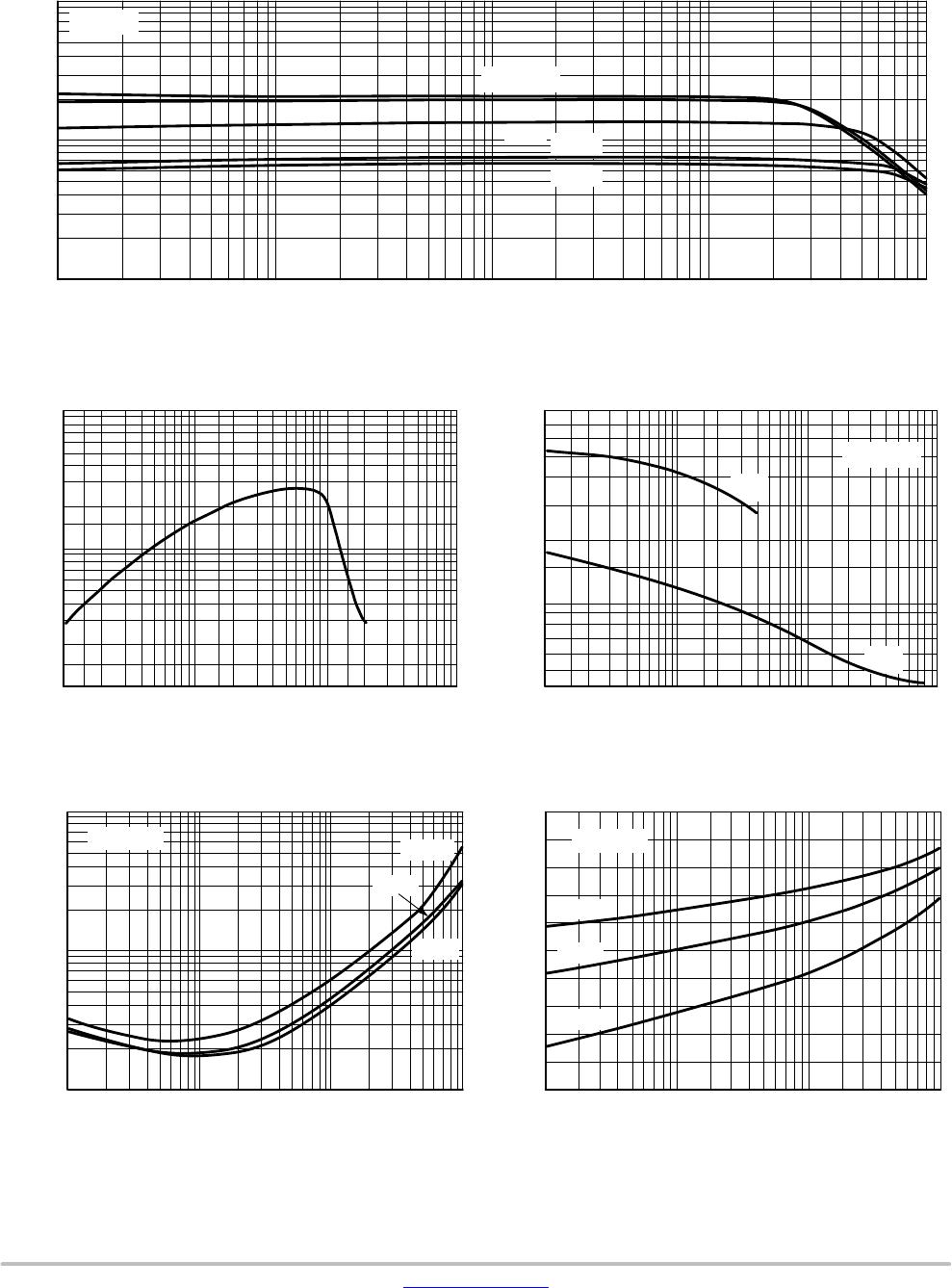
MAXIMUM RATINGS (T
C
= 25°C unless otherwise noted)
Rating
Symbol Value Unit
Collector−Emitter Voltage V
CEO
80 Vdc
Collector−Base Voltage V
CBO
100 Vdc
Emitter−Base Voltage V
EBO
5 Vdc
Collector Current I
C
1 Adc
Total Power Dissipation
@ T
A
= 25°C (Note 1)
Derate above 25°C
P
D
1.5
12
W
mW/°C
Operating and Storage
Temperature Range
T
J
, T
stg
−65 to 150 °C
THERMAL CHARACTERISTICS
Characteristic Symbol Max Unit
Thermal Resistance,
Junction−to−Ambient
(surface mounted)
R
q
JA
83.3 °C/W
Maximum Temperature for
Soldering Purposes
Time in Solder Bath
T
L
260
10
°C
Sec
Stresses exceeding those listed in the Maximum Ratings table may damage the
device. If any of these limits are exceeded, device functionality should not be
assumed, damage may occur and reliability may be affected.
1. Device mounted on a FR−4 glass epoxy printed circuit board 1.575 in x
1.575 in x 0.0625 in; mounting pad for the collector lead = 0.93 sq in.
SOT−223
CASE 318E
STYLE 1
MARKING DIAGRAM
COLLECTOR 2,4
BASE
1
EMITTER 3
MEDIUM POWER NPN SILICON
HIGH CURRENT TRANSISTOR
SURFACE MOUNT
1
2
3
4
www.onsemi.com
See detailed ordering, marking and shipping information in the
package dimensions section on page 2 of this data sheet.
ORDERING INFORMATION
1
AYW
XXXXXG
G
XXXXX = Specific Device Code
A = Assembly Location
Y = Year
W = Work Week
G = Pb−Free Package
(Note: Microdot may be in either location)