VO3062, VO3063
www.vishay.com
Vishay Semiconductors
Rev. 2.0, 18-Apr-13
2
Document Number: 83748
For technical questions, contact: optocoupleranswers@vishay.com
THIS DOCUMENT IS SUBJECT TO CHANGE WITHOUT NOTICE. THE PRODUCTS DESCRIBED HEREIN AND THIS DOCUMENT
ARE SUBJECT TO SPECIFIC DISCLAIMERS, SET FORTH AT www.vishay.com/doc?91000
Notes
• Stresses in excess of the absolute maximum ratings can cause permanent damage to the device. Functional operation of the device is not
implied at these or any other conditions in excess of those given in the operational sections of this document. Exposure to absolute
maximum ratings for extended periods of the time can adversely affect reliability.
(1)
Refer to reflow profile for soldering conditions for surface mounted devices (SMD). Refer to wave profile for soldering conditions for through
hole devices (DIP) “Assembly Instructions” (www.vishay.com/doc?80054
).
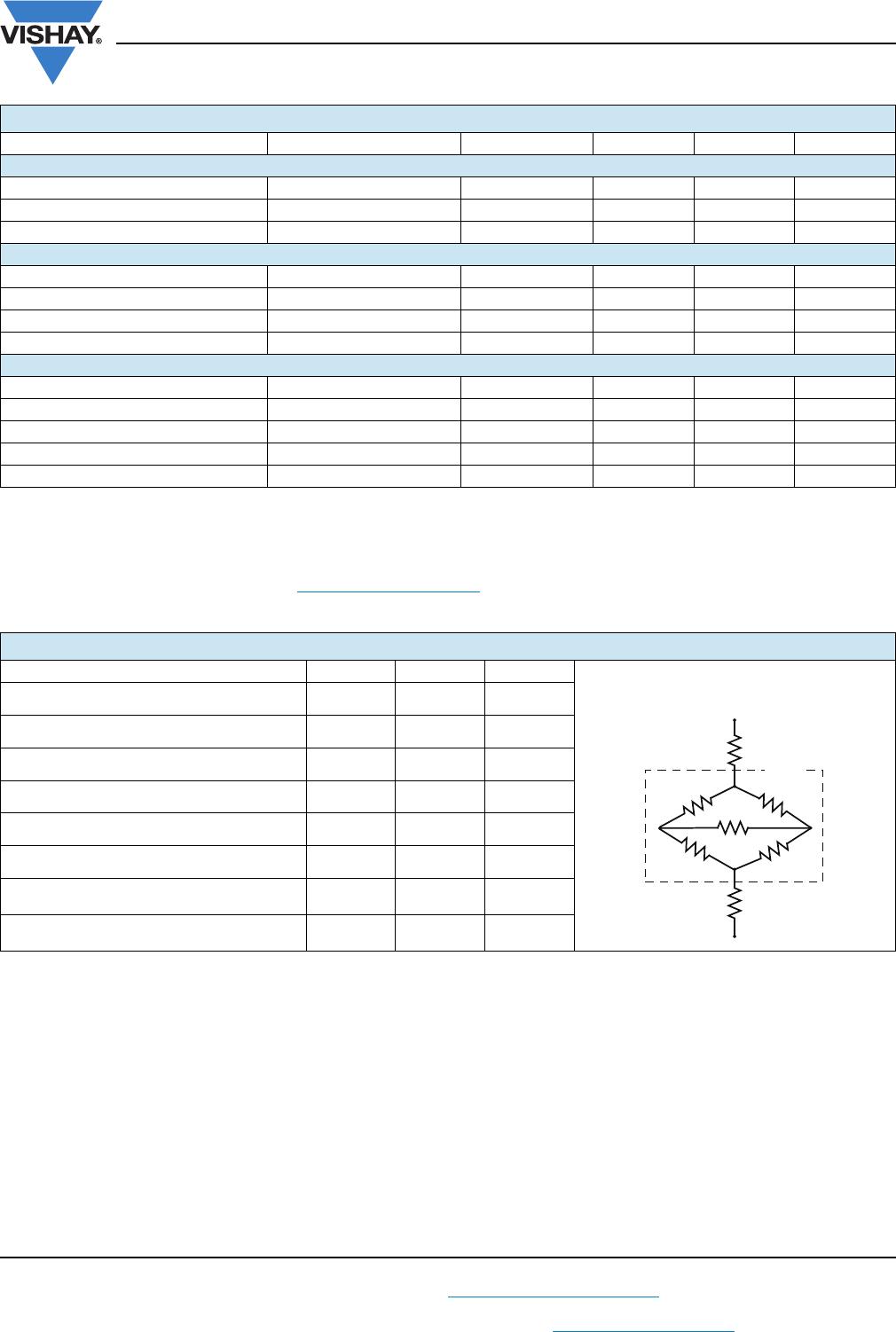
Note
• The thermal model is represented in the thermal network below. Each resistance value given in this model can be used to calculate the
temperatures at each node for a given operating condition. The thermal resistance from board to ambient will be dependent on the type of
PCB, layout and thickness of copper traces. For a detailed explanation of the thermal model, please reference Vishay’s Thermal
Characteristics of Optocouplers application note.
ABSOLUTE MAXIMUM RATINGS (T
amb
= 25 °C, unless otherwise specified)
PARAMETER TEST CONDITION PART SYMBOL VALUE UNIT
INPUT
Reverse voltage V
R
6V
Forward current - continuous I
F
60 mA
Power dissipation P
diss
100 mW
OUTPUT
Off state output terminal voltage VO3062, VO3063 V
DRM
600 V
Peak non-repetitive surge current PW = 100 μs, 120 pps I
TSM
1A
Power dissipation P
diss
200 mW
On-state RMS current I
T(RMS)
100 mA
COUPLER
Isolation test voltage t = 1 s V
ISO
5300 V
RMS
Total power dissipation P
tot
300 mW
Operating temperature range T
amb
- 55 to + 100 °C
Storage temperature range T
stg
- 55 to + 150 °C
Soldering temperature
(1)
maximum 10 s T
sld
260 °C
THERMAL CHARACTERISTICS
PARAMETER SYMBOL VALUE UNIT
Maximum LED junction temperature T
jmax.
125 °C
Maximum output die junction temperature T
jmax.
125 °C
Thermal resistance, junction emitter to board
JEB
150 °C/W
Thermal resistance, junction emitter to case
JEC
139 °C/W
Thermal resistance, junction detector to board
JDB
78 °C/W
Thermal resistance, junction detector to case
JDC
103 °C/W
Thermal resistance, junction emitter to
junction detector
JED
496 °C/W
Thermal resistance, case to ambient
CA
3563 °C/W
T
A
θ
CA
T
C
T
JD
T
JE
T
B
θ
EC
θ
EB
θ
DC
θ
DB
θ
BA
θ
DE
T
A
19996
Package