Isolated Sigma-Delta Modulator
Data Sheet
AD7400
Rev. G Document Feedback
Information furnished by Analog Devices is believed to be accurate and reliable. However, no
responsibility is assumed by Analog Devices for its use, nor for any infringements of patents or other
rights of third parties that may result from its use. Specifications subject to change without notice. No
license is granted by implication or otherwise under any patent or patent rights of Analog Devices.
Trademarks and registered trademarks are the property of their respective owners.
One Technology Way, P.O. Box 9106, Norwood, MA 02062-9106, U.S.A.
Tel: 781.329.4700 ©2006–2013 Analog Devices, Inc. All rights reserved.
Technical Support www.analog.com
FEATURES
10 MHz clock rate
Second-order modulator
16 bits no missing codes
±2 LSB INL typical at 16 bits
3.5 μV/°C maximum offset drift
On-board digital isolator
On-board reference
Low power operation: 18 mA maximum at 5.25 V
−40°C to +105°C operating range
16-lead SOIC package
Safety and regulatory approvals
UL recognition
5000 V rms for 1 minute per UL 1577
CSA Component Acceptance Notice #5A
VDE Certificate of Conformity
DIN V VDE V 0884-10 (VDE V 0884-10):2006-12
V
IORM
= 891 V peak
APPLICATIONS
AC motor controls
Data acquisition systems
A/D + opto-isolator replacements
GENERAL DESCRIPTION
The AD7400
1
is a second-order, sigma-delta (Σ-Δ) modulator
that converts an analog input signal to a high speed, 1-bit data
stream with on-chip digital isolation based on Analog Devices,
Inc. iCoupler® technology. The AD7400 operates from a 5 V
power supply and accepts a differential input signal of ±200 mV
(±320 mV full scale). The analog input is continuously sampled
by the analog modulator, eliminating the need for external
sample-and-hold circuitry. The input information is contained
in the output stream as a density of ones with a data rate of
10 MHz. The original information can be reconstructed with an
appropriate digital filter. The serial I/O can use a 5 V or a 3 V
supply (V
DD2
).
The serial interface is digitally isolated. High speed CMOS,
combined with monolithic air core transformer technology,
means the on-chip isolation provides outstanding performance
characteristics superior to alternatives such as optocoupler
devices. The part contains an on-chip reference. The AD7400 is
offered in a 16-lead SOIC and has an operating temperature
range of −40°C to +105°C.
An external clock version, AD7401, is also available.
1
Protected by U.S. Patents 5,952,849; 6,873,065; and 7,075,329.
FUNCTIONAL BLOCK DIAGRAM
04718-001
V
IN
+
V
DD1
V
DD2
V
IN
Σ- ADC
CONTROL LOGIC
AD7400
B
U
F
T
/
H
REF
UPDATE
GND
1
GND
2
MDAT
MCLKOUT
ENCODE
ENCODE DECODE
DECODE
WATCHDOG
WATCHDOG
UPDATE
Figure 1.
AD7400* PRODUCT PAGE QUICK LINKS
Last Content Update: 02/23/2017
COMPARABLE PARTS
View a parametric search of comparable parts.
EVALUATION KITS
AD7400 Evaluation Board
DOCUMENTATION
Application Notes
AN-0971: Recommendations for Control of Radiated
Emissions with isoPower Devices
AN-1265: Isolated Motor Control Feedback Using the
ADSP-CM402F/ADSP-CM403F/ADSP-CM407F/ADSP-
CM408F SINC Filters and the AD7401A
AN-727: iCoupler® Isolation in RS-485 Applications
AN-740: iCoupler® Isolation in RS-232 Applications
AN-770: iCoupler® Isolation in CAN Bus Applications
AN-793: ESD/Latch-Up Considerations with iCoupler®
Isolation Products
AN-825: Power Supply Considerations in iCoupler®
Isolation Products
AN-913: Isolating I2C Interfaces
Data Sheet
AD7400: Isolated Sigma-Delta Modulator Data Sheet
SOFTWARE AND SYSTEMS REQUIREMENTS
CED1Z FPGA Project for AD7400A with Nios driver
AD7400 and AD7400A Evaluation Software
TOOLS AND SIMULATIONS
AD7400/AD7401 IBIS Model
REFERENCE MATERIALS
Press
Analog Devices Achieves Major Milestone by Shipping 1
Billionth Channel of iCoupler Digital Isolation
Product Selection Guide
Digital Isolator Product Selection and Resource Guide
Technical Articles
Inside iCoupler® Technology:ADuM347x PWM Controller
and Transformer Driver with Quad-Channel Isolators
Design Summary
N
App
kin Note: Lowering the Power of the ADuM524x
Sigma-Delta Conversion Used for Motor Control
DESIGN RESOURCES
AD7400 Material Declaration
PCN-PDN Information
Quality And Reliability
Symbols and Footprints
DISCUSSIONS
View all AD7400 EngineerZone Discussions.
SAMPLE AND BUY
Visit the product page to see pricing options.
TECHNICAL SUPPORT
Submit a technical question or find your regional support
number.
DOCUMENT FEEDBACK
Submit feedback for this data sheet.
This page is dynamically generated by Analog Devices, Inc., and inserted into this data sheet. A dynamic change to the content on this page will not
trigger a change to either the revision number or the content of the product data sheet. This dynamic page may be frequently modified.
AD7400 Data Sheet
Rev. G | Page 2 of 20
TABLE OF CONTENTS
Features .............................................................................................. 1
Applications ....................................................................................... 1
General Description ......................................................................... 1
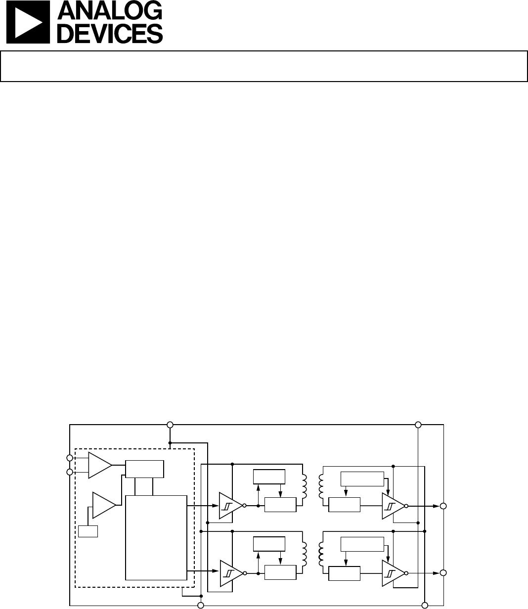
Functional Block Diagram .............................................................. 1
Revision History ............................................................................... 2
Specifications ..................................................................................... 3
Timing Specifications .................................................................. 4
Insulation and Safety-Related Specifications ............................ 5
Regulatory Information ............................................................... 5
DIN V VDE V 0884-10 (VDE V 0884-10) Insulation
Characteristics .............................................................................. 6
Absolute Maximum Ratings ............................................................ 7
ESD Caution .................................................................................. 7
Pin Configuration and Function Descriptions ............................. 8
Typical Performance Characteristics ..............................................9
Terminology .................................................................................... 12
Theory of Operation ...................................................................... 13
Circuit Information .................................................................... 13
Analog Input ............................................................................... 13
Differential Inputs ...................................................................... 14
Digital Filter ................................................................................ 15
Applications Information .............................................................. 17
Grounding and Layout .............................................................. 17
Evaluating the AD7400 Performance ...................................... 17
Insulation Lifetime ..................................................................... 17
Outline Dimensions ....................................................................... 18
Ordering Guide .......................................................................... 18
REVISION HISTORY
6/13—Rev. F to Rev. G
Changes to Figure 12 and Figure 13 ............................................. 10
3/12Rev. E to Rev. F
Changed I
DD1
Parameter from 12 mA to 13 mA, Table 1 ............ 3
7/11Rev. D to Rev. E
Changes to Minimum External Air Gap (Clearance) Parameter,
Table 3 and Minimum External Tracking (Creepage) Parameter,
Table 3 ................................................................................................ 5
Changes to Figure 5; Pin 1 Description, Table 8; and Pin 7
Description, Table 8 .......................................................................... 8
4/11Rev. C to Rev. D
Changes to Dynamic Input Current Parameter, Table 1 ............. 3
1/11Rev. B to Rev. C
Changes to Features Section............................................................ 1
Changes to Input-to-Output Momentary Withstand Voltage
Parameter, Table 3, UL Column, Table 4, and Note 1, Table 4 .......... 5
Changes to Ordering Guide ..................................................................... 18
9/07Rev. A to Rev. B
Updated VDE Certification Throughout ...................................... 1
Changes to Table 6 ............................................................................. 7
12/06Rev. 0 to Rev. A
Changes to Features .......................................................................... 1
Changes to Table 6 ............................................................................. 7
Changes to Analog Input Section ................................................. 13
Changes to Figure 26 ...................................................................... 15
1/06Revision 0: Initial Version

AD7400YRWZ-REEL

Mfr. #:
Manufacturer:
Analog Devices Inc.
Description:
Data Acquisition ADCs/DACs - Specialized Isolated Modulator
Lifecycle:
New from this manufacturer.
Delivery:
DHL FedEx Ups TNT EMS
Payment:
T/T Paypal Visa MoneyGram Western Union

Products related to this Datasheet