© Semiconductor Components Industries, LLC, 2011
October, 2011 − Rev. 5
1 Publication Order Number:
NTS4001N/D
NTS4001N, NVS4001N
Small Signal MOSFET
30 V, 270 mA, Single N−Channel, SC−70
Features
• Low Gate Charge for Fast Switching
• Small Footprint − 30% Smaller than TSOP−6
• ESD Protected Gate
• AEC−Q101 Qualified and PPAP Capable − NVS4001N
• These Devices are Pb−Free and are RoHS Compliant
Applications
• Low Side Load Switch
• Li−Ion Battery Supplied Devices − Cell Phones, PDAs, DSC
• Buck Converters
• Level Shifts
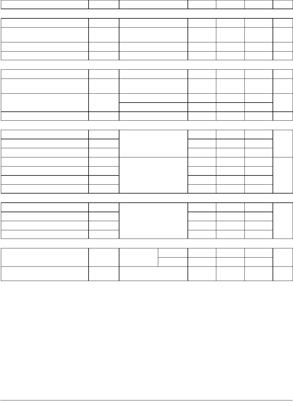
MAXIMUM RATINGS (T
J
= 25°C unless otherwise stated)
Parameter
Symbol Value Units
Drain−to−Source Voltage V
DSS
30 V
Gate−to−Source Voltage V
GS
±20 V
Continuous Drain
Current (Note 1)
Steady
State
T
A
= 25 °C
I
D
270
mA
T
A
= 85 °C 200
Power Dissipation
(Note 1)
Steady
State
T
A
= 25 °C P
D
330 mW
Pulsed Drain Current
t =10 ms
I
DM
800 mA
Operating Junction and Storage Temperature T
J
, T
STG
−55 to
150
°C
Source Current (Body Diode) I
S
270 mA
Lead Temperature for Soldering Purposes
(1/8” from case for 10 s)
T
L
260 °C
Stresses exceeding Maximum Ratings may damage the device. Maximum
Ratings are stress ratings only. Functional operation above the Recommended
Operating Conditions is not implied. Extended exposure to stresses above the
Recommended Operating Conditions may affect device reliability.
1. Surface mounted on FR4 board using 1 in sq. pad size
(Cu area = 1.127 in sq. [1 oz] including traces).
Device Package Shipping
†
ORDERING INFORMATION
(Top View)
SC−70 / SOT−323
CASE 419
STYLE 8
MARKING DIAGRAM &
PIN ASSIGNMENT
2
1
http://onsemi.com
TD = Device Code
M = Date Code*
G = Pb−Free Package
SC−70/SOT−323 (3 LEADS)
Drain
Gate
3
1
2
V
(BR)DSS
R
DS(on)
TYP I
D
Max
30 V
1.0 W @ 4.0 V
1.5 W @ 2.5 V
270 mA
NTS4001NT1G
SC−70
(Pb−Free)
3000 / Tape & Reel
TD M G
G
Source
3
1
2
3
GS
D
(Note: Microdot may be in either location)
*Date Code orientation may vary depending
upon manufacturing location.
†For information on tape and reel specifications,
including part orientation and tape sizes, please
refer to our Tape and Reel Packaging Specification
Brochure, BRD8011/D.
NVS4001NT1G
SC−70
(Pb−Free)
3000 / Tape & Reel