REV. A
AD7390/AD7391
–4–
PIN DESCRIPTIONS
Pin No. Name Function
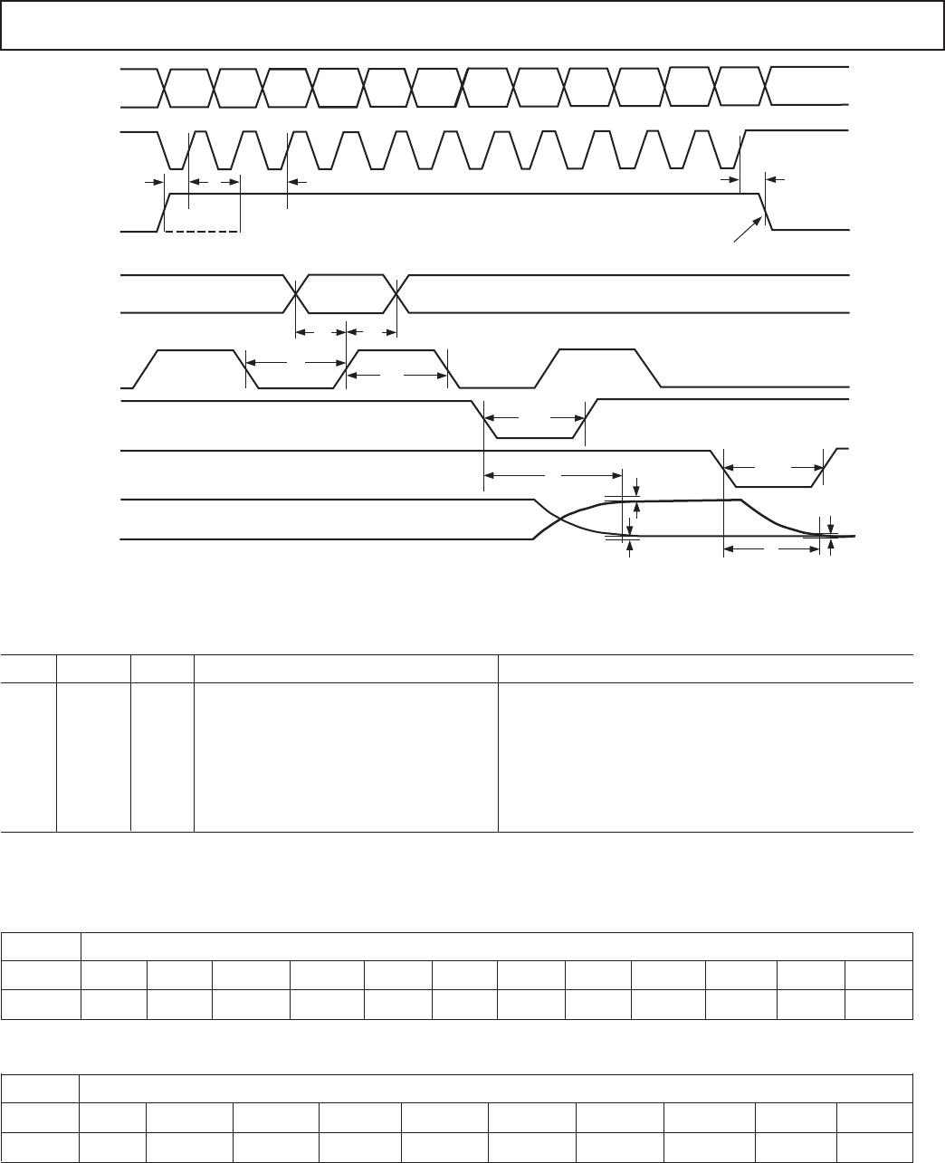
1 LD Load Strobe. Transfers shift register
data to DAC register while active low.
See truth table for operation.
2 CLK Clock Input. Positive edge clocks data
into shift register.
3 SDI Serial Data Input. Data loads directly
into the shift register.
4 CLR Resets DAC register to zero condition.
Active low input.
5 GND Analog and Digital Ground.
6V
OUT
DAC Voltage Output. Full-scale output
1 LSB less than reference input voltage REF.
7V
DD
Positive Power Supply Input. Specified
range of operation 2.7 V to 5.5 V.
8V
REF
DAC Reference Input Pin. Establishes
DAC full-scale voltage.
ABSOLUTE MAXIMUM RATINGS*
V
DD
to GND . . . . . . . . . . . . . . . . . . . . . . . . . . . 0.3 V, 8 V
V
REF
to GND . . . . . . . . . . . . . . . . . . . . . . 0.3 V, V
DD
0.3 V
Logic Inputs to GND . . . . . . . . . . . . . . . . . . . . .0.3 V, 8 V
V
OUT
to GND . . . . . . . . . . . . . . . . . . . . 0.3 V, V
DD
0.3 V
I
OUT
Short Circuit to GND . . . . . . . . . . . . . . . . . . . . . . 50 mA
Package Power Dissipation . . . . . . . . . . . . . (T
J MAX
T
A
)/θ
JA
Thermal Resistance θ
JA
8-Lead Plastic DIP Package (N-8) . . . . . . . . . . . . . 103°C/W
8-Lead SOIC Package (SO-8) . . . . . . . . . . . . . . . . 158°C/W
TSSOP-8 Package (RU-8) . . . . . . . . . . . . . . . . . . . 240°C/W
Maximum Junction Temperature (T
J MAX
) . . . . . . . . . . 150°C
Operating Temperature Range . . . . . . . . . . 40°C to 85°C
AD7391AR . . . . . . . . . . . . . . . . . . . . . . . . 40°C to 125°C
Storage Temperature Range . . . . . . . . . . . 65°C to 150°C
Lead Temperature (Soldering, 10 secs) . . . . . . . . . . . . . 300°C
*Stresses above those listed under Absolute Maximum Ratings may cause perma-
nent damage to the device. This is a stress rating only; functional operation of the
device at these or any other conditions above those indicated in the operational
specification is not implied. Exposure to the above maximum rating conditions for
extended periods may affect device reliability.
DAC
REGISTER
RESET
LOAD
CLK
12-BIT AD7390*
SHIFT REGISTER
D
CLR
LD
CLK
SDI
12
*AD7391 HAS A 10-BIT SHIFT REGISTER
Figure 3. Digital Control Logic
PIN CONFIGURATIONS
TOP VIEW
(Not to
Scale)
1
2
3
4
8
7
6
5
TOP VIEW
(Not to Scale)
8
7
6
5
1
2
3
4
TOP VIEW
(Not to Scale)
8
7
6
5
1
2
3
4
LD
CLK
CLR
SDI
GND
V
REF
V
DD
V
OUT
TSSOP-8
SO-8
P-DIP-8
CAUTION
ESD (electrostatic discharge) sensitive device. Electrostatic charges as high as 4000 V readily
accumulate on the human body and test equipment and can discharge without detection. Although
the AD7390/AD7391 features proprietary ESD protection circuitry, permanent damage may occur
on devices subjected to high-energy electrostatic discharges. Therefore, proper ESD precautions
are recommended to avoid performance degradation or loss of functionality.
WARNING!
ESD SENSITIVE DEVICE
ORDERING GUIDE
1
Temperature Package Package Top Number of Devices
Model Resolution Range Description Option Mark
2
Per Container
AD7390AN 12 40°C to 85°C 8-Lead P-DIP N-8 AD7390
2
50
AD7390AR 12 40°C to 85°C 8-Lead SOIC SO-8 AD7390
3
196
AD7390AR-REEL7 12 40°C to 85°C 8-Lead SOIC SO-8 AD7390
3
1000
AD7391AN 10 40°C to 85°C 8-Lead P-DIP N-8 AD7391
2
50
AD7391AR 10 40°C to 125°C 8-Lead SOIC SO-8 AD7391
3
196
AD7391SR 10 55°C to 125°C 8-Lead SOIC SO-8 AD7391
3
39
AD7391ARU-REEL 10 40°C to 85°C TSSOP-8 RU-8 AD7391A
4
2500
NOTES
1
The AD7390 contains 588 transistors. The die size measures 70 mm 68 mm.
2
Line 1 contains ADI logo symbol and part number. Line 2 contains grade and date code YWW. Line 3 contains the letter G plus the 4-digit lot number.
3
Line 1 contains part number. Line 2 contains grade and date code YWW. Line 3 contains the letter G plus the 4-digit lot number and the ADI logo symbol.
4
Line 1 contains the date code YWW. Line 2 contains the 4-digit part number plus grade.