ADM1813-5ARTZ-RL7

ADM1810 to ADM1813/ADM1815 to ADM1818 Data Sheet
Rev. F | Page 4 of 12
ABSOLUTE MAXIMUM RATINGS
T
A
= 25°C, unless otherwise noted.
Table 2.
Parameter Rating
V
CC
−0.3 V to +6.0 V
Input Current 20 mA
Operating Temperature Range −40°C to +105°C
Storage Temperature Range −65°C to +150°C
θ
JA
Thermal Impedance, SOT-23 270°C/W
θ
JA
Thermal Impedance, SC70 146°C/W
Lead Temperature (Soldering, 10 sec) 300°C
Vapor Phase (60 sec) 215°C
Infrared (15 sec) 220°C
Stresses above those listed under Absolute Maximum Ratings
may cause permanent damage to the device. This is a stress
rating only; functional operation of the device at these or any
other conditions above those indicated in the operational
section of this specification is not implied. Exposure to absolute
maximum rating conditions for extended periods may affect
device reliability.
ESD CAUTION
Data Sheet ADM1810 to ADM1813/ADM1815 to ADM1818
Rev. F | Page 5 of 12
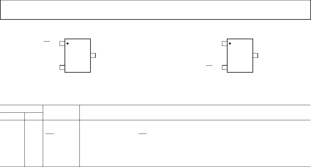
PIN CONFIGURATIONS AND FUNCTION DESCRIPTIONS
Figure 2. 3-Lead SOT-23 Pin Configuration
Figure 3. 3-Lead SC70 Pin Configuration
Table 3. Pin Function Descriptions
Pin No.
Mnemonic Description
SOT-23
SC70
1 2 RST
Active High Reset Output. RST remains high while V
CC
is below the reset threshold and remains high for
150 ms typical after V
CC
rises above the reset threshold. Applies to the ADM1812 and ADM1817 only.
RST Active Low Reset Output. RST remains low while V
CC
is below the reset threshold and remains low for
150 ms typical after V
CC
rises above the reset threshold. Applies to the ADM1810, ADM1811, ADM1813,
ADM1815, ADM1816, and ADM1818 only.
2 1 V
CC
Supply Voltage. The supply voltage being monitored.
3 3 GND Ground. 0 V ground reference for all signals.
00064-002
ADM181x
TOP VIEW
(Not to Scale)
RST/RST
1
V
CC
2
GND
3
00064-014
ADM181x
TOP VIEW
(Not to Scale)
1
V
CC
2
GND
3
RST/RST
ADM1810 to ADM1813/ADM1815 to ADM1818 Data Sheet
Rev. F | Page 6 of 12
TYPICAL PERFORMANCE CHARACTERISTICS
Figure 4. Supply Current vs. Temperature
Figure 5. Power-Down Reset Delay vs. Temperature
Figure 6. Power-Up Reset Timeout vs. Temperature
Figure 7. Normalized Reset Threshold vs. Temperature
Figure 8. Maximum Transient Duration Without Causing a Reset Pulse vs.
Reset Comparator Overdrive
10
0
2
4
6
8
40 120100
85
7050
30
200
–20
00064-003
TEMPERATURE (°C)
I
CC
(µA)
I
CC
@V
CC
= 3V
I
CC
@V
CC
= 5.5V
900
800
700
600
500
400
300
200
100
0
00064-004
TEMPERATURE (°C)
POWER-DOWN RESET DELAY (µs)
–40 1201008570
503020
0–20
VOD = 20mV
VOD = 125mV
VOD = 200mV
380
370
360
350
340
330
320
310
300
290
00064-005
TEMPERATURE (°C)
POWER-UP RESET TIMEOUT (ms)
40 12010085705030200
20
1.011
0.995
0.997
0.999
1.001
1.003
1.005
1.007
1.009
–40
120100
85
7050
30
200
–20
00064-006
TEMPERATURE (°C)
NORMALIZED RESET THRESHOLD
DEVIATION (RISE)
DEVIATION (FALL)
60
0
10
20
30
40
50
10 1000800600400200100
806040
30
00064-007
V
TH
V
CC
(mV)
MAXIMUM TRANSIENT (µs)

ADM1813-5ARTZ-RL7

Mfr. #:
Manufacturer:
Analog Devices Inc.
Description:
Supervisory Circuits RESET GENERATOR I.C.
Lifecycle:
New from this manufacturer.
Delivery:
DHL FedEx Ups TNT EMS
Payment:
T/T Paypal Visa MoneyGram Western Union