P4KE6.8A thru P4KE540A
www.vishay.com
Vishay General Semiconductor
Revision: 18-Sep-12
1
Document Number: 88365
For technical questions within your region: DiodesAmericas@vishay.com
, DiodesAsia@vishay.com, DiodesEurope@vishay.com
THIS DOCUMENT IS SUBJECT TO CHANGE WITHOUT NOTICE. THE PRODUCTS DESCRIBED HEREIN AND THIS DOCUMENT
ARE SUBJECT TO SPECIFIC DISCLAIMERS, SET FORTH AT www.vishay.com/doc?91000
TRANSZORB
®
Transient Voltage Suppressors
DEVICES FOR BI-DIRECTION APPLICATIONS
For bi-directional types, use CA suffix (e.g. P4KE440CA).
Electrical characteristics apply in both directions.
FEATURES
• Glass passivated chip junction
• Available in uni-directional and bi-directional
• 400 W peak pulse power capability with a
10/1000 μs waveform, repetitive rate (duty
cycle): 0.01 %
• Excellent clamping capability
• Very fast response time
• Low incremental surge resistance
• Solder dip 275 °C max. 10 s, per JESD 22-B106
• AEC-Q101 qualified
• Material categorization: For definitions of compliance
please see www.vishay.com/doc?99912
TYPICAL APPLICATIONS
Use in sensitive electronics protection against voltage
transients induced by inductive load switching and lighting
on ICs, MOSFET, signal lines of sensor units for consumer,
computer, industrial, automotive, and telecommunication.
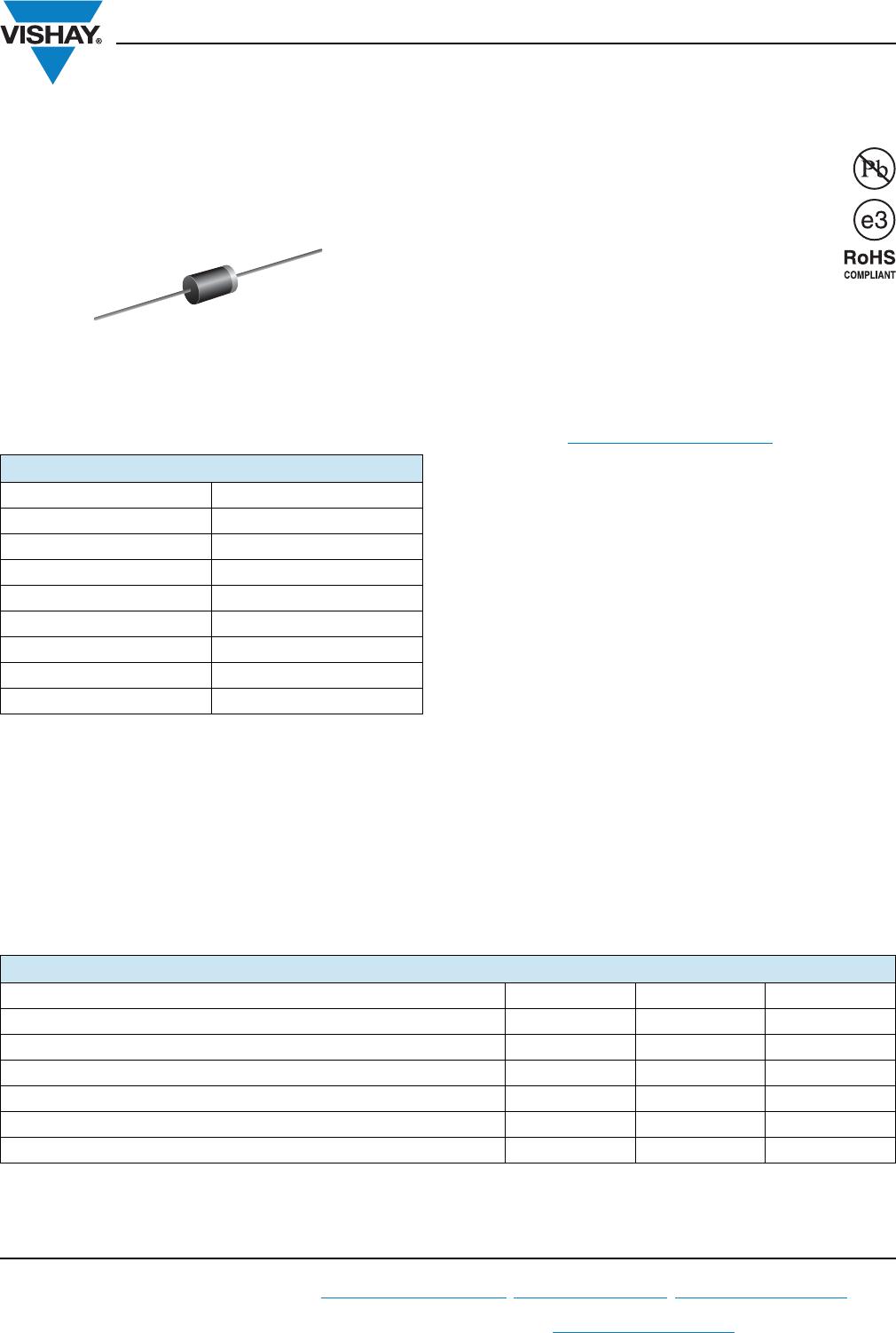
MECHANICAL DATA
Case: DO-204AL, molded epoxy body over passivated chip
Molding compound meets UL 94 V-0 flammability rating
Base P/N-E3 - RoHS-compliant, commercial grade
Base P/NHE3 - RoHS-compliant, AEC-Q101 qualified
Terminals: Matte tin plated leads, solderable per
J-STD-002 and JESD 22-B102
E3 suffix meets JESD 201 class 1A whisker test, HE3 suffix
meets JESD 201 class 2 whisker test
Note
• P4KE250CA to P4KE540A and P4KE250A to P4KE440CA for
commercial grade only
Polarity: For uni-directional types the color band denotes
cathode end, no marking on bi-directional types
Notes
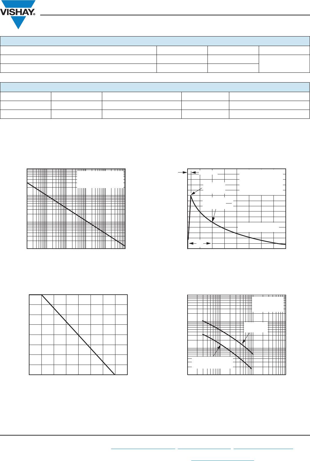
(1)
Non-repetitive current pulse, per fig. 3 and derated above T
A
= 25 °C per fig. 2
(2)
8.3 ms single half-sine wave or equivalent square wave, duty cycle = 4 pulses per minute maximum
(3)
V
F
= 3.5 V for P4KE220A and below; V
F
= 5.0 V for P4KE250A and above
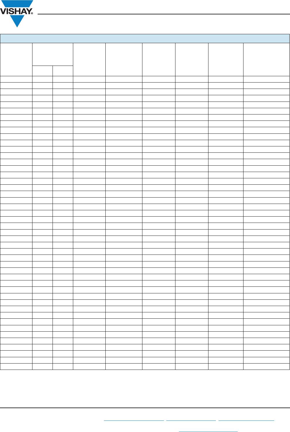
PRIMARY CHARACTERISTICS
V
WM
5.8 V to 459 V
V
BR
uni-directional 6.8 V to 540 V
V
BR
bi-directional 6.8 V to 440 V
P
PPM
400 W
P
D
1.5 W
I
FSM
(uni-directional only) 40 A
T
J
max. 175 °C
Polarity Uni-directional, bi-directional
Package DO-204AL (DO-41)
MAXIMUM RATINGS (T
A
= 25 °C unless otherwise noted)
PARAMETER SYMBOL LIMIT UNIT
Peak pulse power dissipation with a 10/1000 μs waveform
(1)
(fig.1) P
PPM
400 W
Peak pulse current with a 10/1000 μs waveform
(1)
I
PPM
See next table A
Power dissipation on infinite heatsink at T
L
= 75 °C (fig. 5) P
D
1.5 W
Peak forward surge current 8.3 ms single half-sine wave uni-directional only
(2)
I
FSM
40 A
Maximum instantaneous forward voltage at 25 A for uni-directional only
(3)
V
F
3.5/5.0 V
Operating junction and storage temperature range T
J
, T
STG
- 55 to + 175 °C