© 2011 IXYS All rights reserved
2 - 4
20110119a
FII 40-06D
IXYS reserves the right to change limits, test conditions and dimensions.
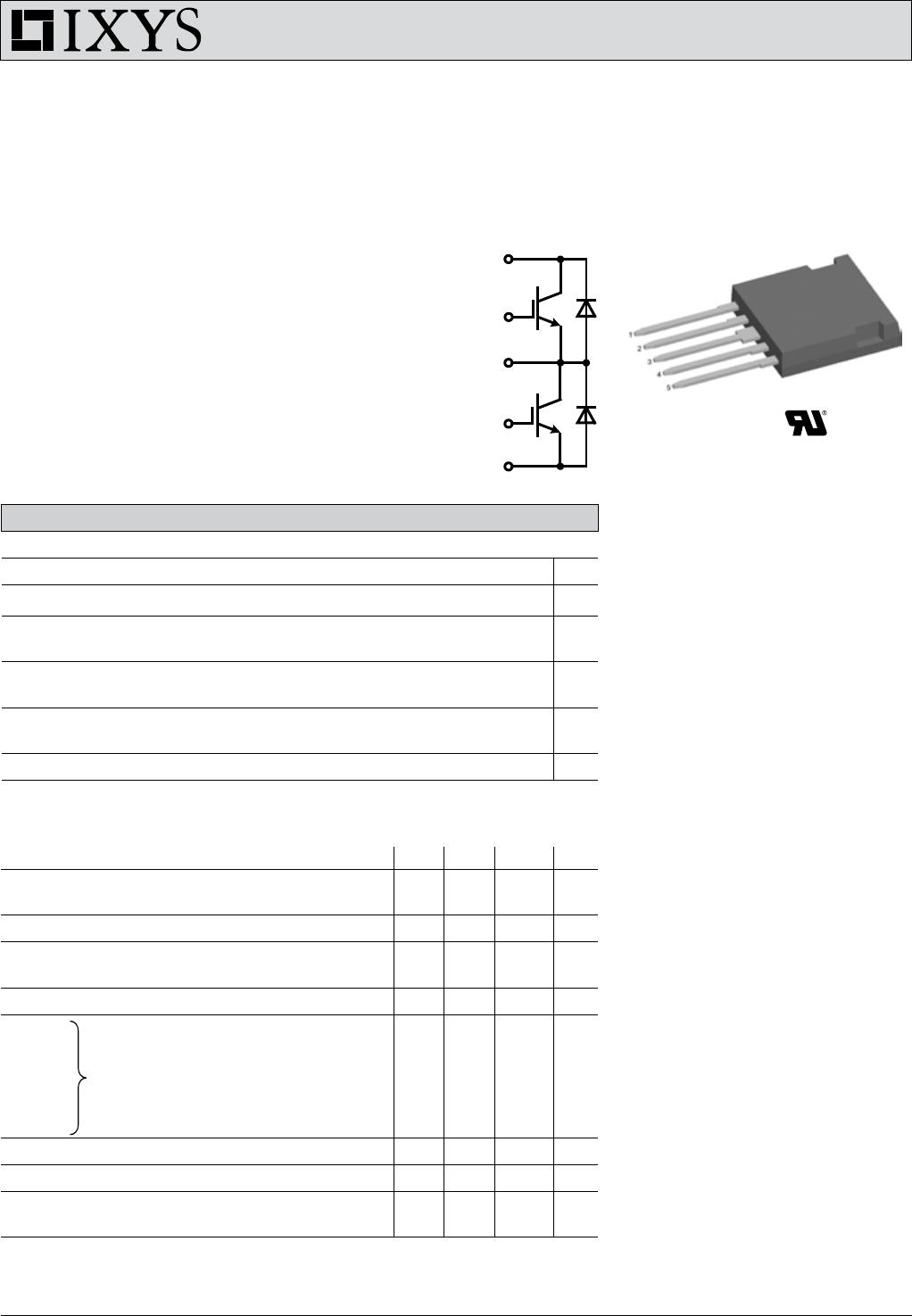
Diode
Symbol Conditions
Maximum Ratings
V
RRM
T
VJ
= 25°C to 150°C 600 V
I
F25
I
F90
T
C
= 25°C
T
C
= 90°C
30
15
A
A
Component
Symbol Conditions Maximum Ratings
T
VJ
T
stg
operating -55...+150
-55...+125
°C
°C
V
ISOL
I
ISOL
< 1 mA; 50/60 Hz; t = 1 s 2500 V~
F
C
Mounting force with clip 20...120 Nm
Symbol Conditions Characteristic Values
min. typ. max.
C
P
coupling capacity between shorted
pins and mounting tab in the case
40 pF
d
S
, d
A
d
S
, d
A
pin - pin
pin - backside metal
1.7
5.5
mm
mm
Weight
6 g
Symbol Conditions Characteristic Values
min. typ. max.
V
F
I
F
= 25 A T
VJ
= 25°C
T
VJ
= 125°C
2.5
1.7
2.8 V
V
I
RM
t
rr
I
F
= 15 A; di
F
/dt = -400 A/µs;
V
R
= 300 V; V
GE
= 0 V; T
VJ
= 125°C
7
50
A
ns
R
thJC
R
thJH
(per diode)
with heatsink compound 4.6
2.3 K/W
K/W
b4
4x e
E
W
A
A2
A1
C
b2
b
E1
D1
D2
L1
L
D
R
Q
1 2 53 4
MIN MAX MIN MAX
A 4.83 5.21 0.190 0.205
A1 2.59 3.00 0.102 0.118
A2 1.17 2.16 0.046 0.085
b 1.14 1.40 0.045 0.055
b2 1.47 1.73 0.058 0.068
b4 2.54 2.79 0.100 0.110
C 0.51 0.74 0.020 0.029
D 20.80 21.34 0.819 0.840
D1 14.99 15.75 0.590 0.620
D2 1.65 2.03 0.065 0.080
E 19.56 20.29 0.770 0.799
E1 16.76 17.53 0.660 0.690
e
L 19.81 21.34 0.780 0.840
L1 2.11 2.59 0.083 0.102
Q 5.33 6.20 0.210 0.244
R
2.54
4.57 0.100 0.180
W
―
0.10
―
0.004
DIM.
MILLIMETER INCHES
3.81 BSC 0.15 BSC
Die konvexe Form des Substrates ist typ. < 0.05 mm über
der Kunststoffoberfläche der Bauteilunterseite
The convex bow of substrate is typ. < 0.05 mm over plastic
surface level ofdevice bottom side