ICS8442BY REVISION A NOVEMBER 18, 2013 8 ©2013 Integrated Device Technology, Inc.
ICS8442B Data Sheet 700MHz, CRYSTAL OSCILLATOR-TO-DIFFERENTIAL LVDS FREQUENCY SYNTHESIZER
STORAGE AREA NETWORKS
A variety of technologies are used for interconnection of the
elements within a SAN. The tables below lists the common fre-
Table 8. Common SANs Application Frequencies
Table 9. Configuration Details for SANs Applications
APPLICATION INFORMATION
ygolonhceTtcennocretnIetaRkcolC
SEDRESotycneuqerFecnerefeR
)zHM(
ycneuqerFlatsyrC
)zHM(
tenrehtEtibagiGzHG52
.152.651,052,52152135.91,52
lennahCerbiF
zHG5260.11CF
zHG0521.22CF
5218.231,521.35,52.60152,5265106.61
dnabin
ifnIzHG5.2052,52152
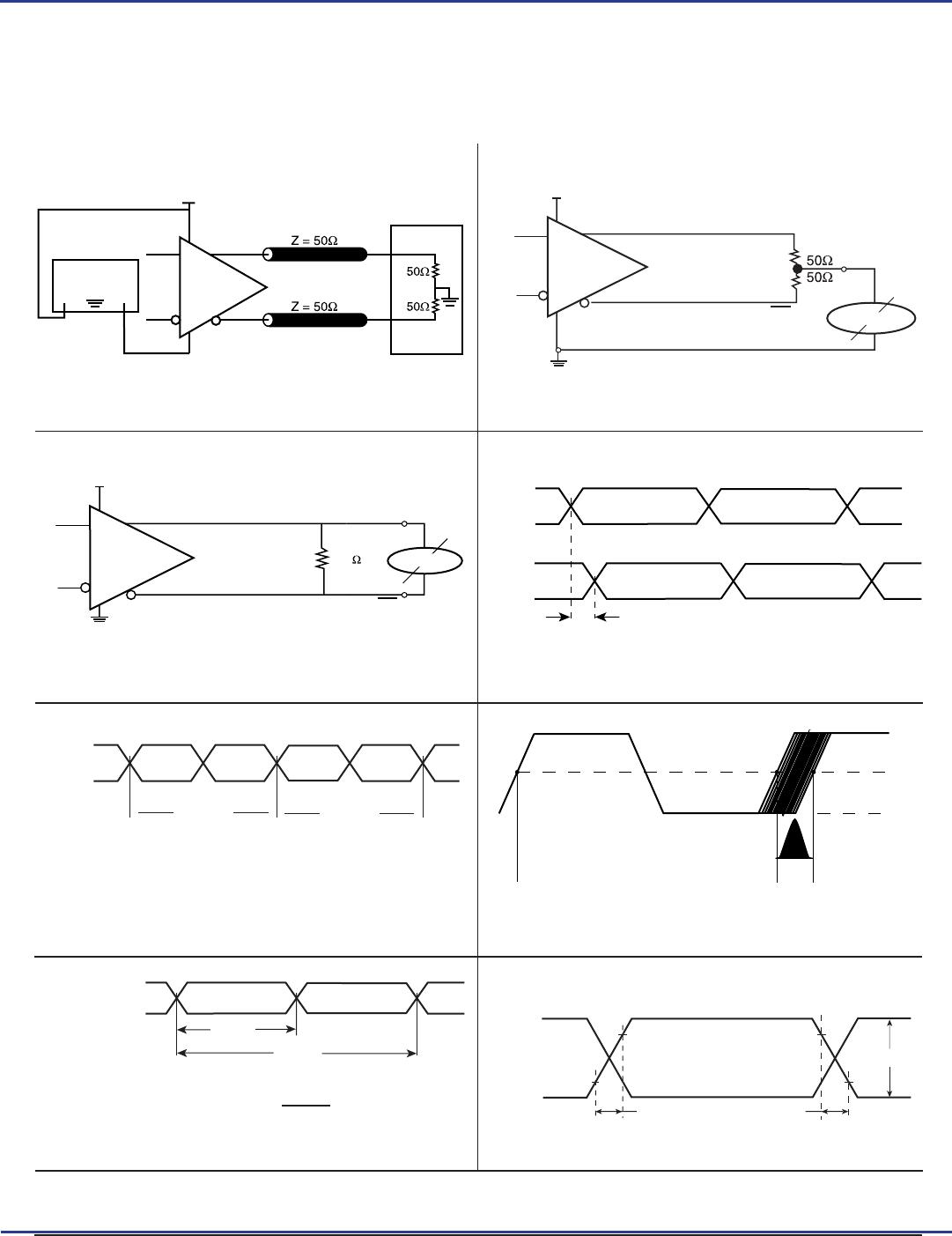
As in any high speed analog circuitry, the power supply pins
are vulnerable to random noise. The ICS8442B provides
separate power supplies to isolate any high switching noise
from the outputs to the internal PLL. V
DD
and V
DDA
, should
be individually connected to the power supply plane through
vias, and bypass capacitors should be used for each pin. To
achieve optimum jitter performance, better power supply
isolation is required.
Figure 2
illustrates how a 10Ω along
|with a 10μF and a .01μF bypass capacitor should be
connected to each V
DDA
pin.
POWER SUPPLY FILTERING T ECHNIQUES
FIGURE 2. POWER SUPPLY FILTERING
10Ω
V
DDA
10μF
.01μF
3.3V
.01μF
V
DD
tcennocretnI
ygolonhceT
ycneuqerFlatsyrC
)zHM(
B2448SCI
ycneuqerFtuptuO
SEDRESot
)zHM(
B2448SCI
sgnitteSN&M
8M7M6
M5M4M3M2M1M0M1N0N
tenrehtEtibagiG
52521 000010 10010
52052 000010 10001
5252.651 00001100 110
52135.9152.651 000100000 10
1lennahCrebiF
52521.35 00001000 111
5252.601 00001000 110
2lennahCrebiF5265106.615
218.231 000100000 10
dnabinifnI
52521 000010 10010
52052 000010 10001
quencies used as well as the settings for the ICS8442B to
generate the appropriate frequency.