MCK12140DG

© Semiconductor Components Industries, LLC, 2006
July, 2006 Rev. 9
1 Publication Order Number:
MCH12140/D
MCH12140, MCK12140
Phase-Frequency Detector
Description
The MCH/K12140 is a phase frequencydetector intended for
phaselocked loop applications which require a minimum amount of
phase and frequency difference at lock. When used in conjunction
with high performance VCO such as the MC100EL1648, a high
bandwidth PLL can be realized. The device is functionally compatible
with the MC12040 phasefrequency detector with the maximum
frequency extending to 800 MHz.
When the Reference (R) and VCO (V) inputs are unequal in
frequency and/or phase, the differential UP (U) and DOWN (D)
outputs will provide pulse streams which when subtracted and
integrated provide an error voltage for control of a VCO. See
AND8040 for further information. The device is packaged in a small
outline, surface mount 8lead SOIC package. There are two versions
of the device to provide I/O compatibility to the two existing ECL
standards. The MCH12140 is compatible with MECL 10H logic
levels while the MCK12140 is compatible to 100 K ECL logic levels.
This device can also be used in +5.0 V systems. See AND8020 for
termination information
Features
800 MHz Typical Bandwidth
Small Outline 8-Lead SOIC Package
75 kW Internal Input Pulldown Resistors
>1000 V ESD Protection
PbFree Packages are Available
For proper operation, the input edge rate of the R and V inputs
should be less than 5.0 ns.
Figure 1. Logic Diagram
SQ
R
R
RQ
V
U (fR > fV)
U (fR > fV)
D (fV > fR)
D (fV > fR)
S
SOIC8
D SUFFIX
CASE 751
PIN CONNECTIONS
MARKING
DIAGRAM
x = H or K
A = Assembly Location
L = Wafer Lot
Y = Year
W = Work Week
G = PbFree Package
V
CC
8
U
U
D
D
R
V
V
EE
7
6
5
1
2
3
4
(Top View)
http://onsemi.com
x140
ALYW
G
1
8
See detailed ordering and shipping information in the package
dimensions section on page 4 of this data sheet.
ORDERING INFORMATION
1
8
MCH12140, MCK12140
http://onsemi.com
2
Table 1. TRUTH TABLE*
Input Output Input Output
R V U D U D R V U D U D
0
0
1
0
0
1
1
1
X
X
X
X
X
X
X
X
X
X
X
X
X
X
X
X
1
1
1
1
1
0
1
0
0
0
0
0
0
0
1
1
1
1
1
1
1
1
0
0
1
0
1
1
1
1
1
0
1
1
1
1
0
0
0
0
0
0
0
0
1
1
1
1
1
0
1
1
1
1
0
0
0
1
1
0
1
1
1
0
0
1
*This is not strictly a functional table; i.e., it does not cover all possible modes of operation. However, it gives a sufficient number of tests to ensure
that the device will function properly.
Table 2. HSERIES DC CHARACTERISTICS (V
EE
= V
EE
(min) V
EE
(max); V
CC
= GND (Note 1), unless otherwise noted.)
Symbol Characteristic
40°C 0°C 25°C 70°C
Unit
Min Max Min Max Min Max Min Max
V
OH
Output HIGH Voltage 1080 890 1020 840 980 810 910 720 mV
V
OL
Output LOW Voltage 1950 1650 1950 1630 1950 1630 1950 1595 mV
V
IH
Input HIGH Voltage 1230 890 1170 840 1130 810 1060 720 mV
V
IL
Input LOW Voltage 1950 1500 1950 1480 1950 1480 1950 1445 mV
I
IL
Input LOW Current 0.5 0.5 0.5 0.3
mA
Table 3. KSERIES DC CHARACTERISTICS (V
EE
= V
EE
(min) V
EE
(max); V
CC
= GND (Note 2), unless otherwise noted.)
Symbol Characteristic
40°C 0°C to 70°C
Condition Unit
Min Typ Max Min Typ Max
V
OH
Output HIGH Voltage 1085 1005 880 1025 955 880 V
IN
= V
IH
(max) mV
V
OL
Output LOW Voltage 1830 1695 1555 1810 1705 1620 or V
IL
(min) mV
V
OHA
Output HIGH Voltage 1095 1035 V
IN
= V
IH
(min) mV
V
OLA
Output LOW Voltage 1555 1610 or V
IL
(max) mV
V
IH
Input HIGH Voltage 1165 880 1165 880 mV
V
IL
Input LOW Voltage 1810 1475 1810 1475 mV
I
IL
Input LOW Current 0.5 0.5 V
IN
= V
IL
(max)
mA
MCH12140, MCK12140
http://onsemi.com
3
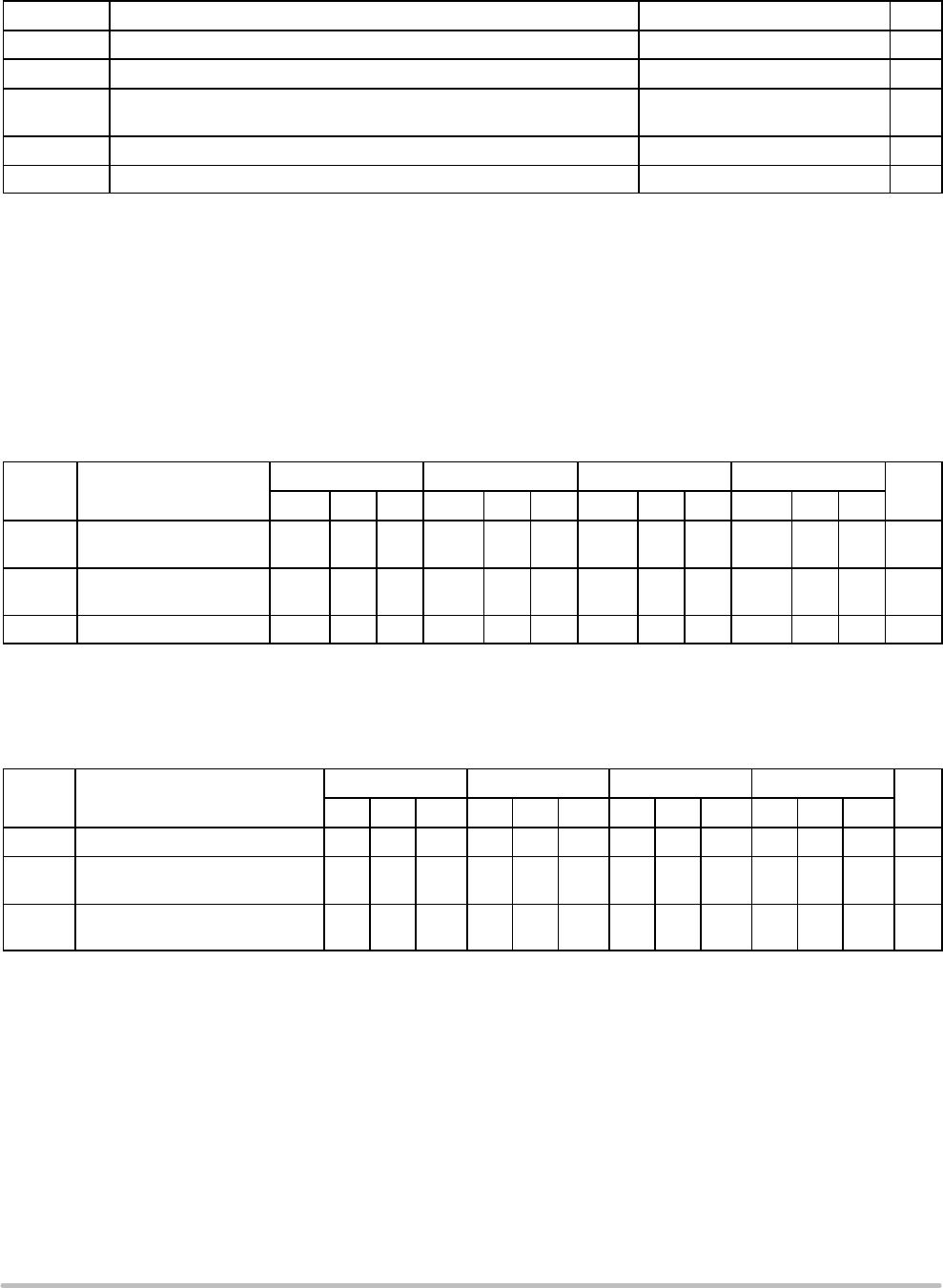
Table 4. MAXIMUM RATINGS
Symbol Rating Value Unit
V
EE
Power Supply (V
CC
= 0 V) 8.0 to 0 VDC
V
I
Input Voltage (V
CC
= 0 V) 0 to 6.0 VDC
I
out
Output Current Continuous
Surge
50
100
mA
T
A
Operating Temperature Range 40 to +70 °C
V
EE
Operating Range (Note 3) 5.7 to 4.2 V
Stresses exceeding Maximum Ratings may damage the device. Maximum Ratings are stress ratings only. Functional operation above the
Recommended Operating Conditions is not implied. Extended exposure to stresses above the Recommended Operating Conditions may affect
device reliability.
NOTE: ESD data available upon request.
1. 10H circuits are designed to meet the DC specifications shown in the table after thermal equilibrium has been established. The circuit is in
a test socket or mounted on a printed circuit board and transverse airflow greater than 500 lfpm is maintained. Outputs are terminated through
a 50 W resistor to 2.0 V except where otherwise specified on the individual data sheets.
2. This table replaces the three tables traditionally seen in ECL 100 K data books. The same DC parameter values at V
EE
= 4.5 V now apply
across the full V
EE
range of 4.2 V to 5.5 V. Outputs are terminated through a 50 W resistor to 2.0 V except where otherwise specified
on the individual data sheets.
3. Parametric values specified at: HSeries: 4.20 V to 5.50 V
KSeries: 4.94 V to 5.50 V
Table 5. DC CHARACTERISTICS (V
EE
= V
EE
(min) V
EE
(max); V
CC
= GND, unless otherwise noted.)
Symbol Characteristic
40°C 0°C 25°C 70°C
Unit
Min Typ Max Min Typ Max Min Typ Max Min Typ Max
I
EE
Power Supply Current H
K
45
45
38
38
45
45
52
52
38
38
45
45
52
52
38
42
45
50
52
58
mA
V
EE
Power Supply Voltage H
K
4.75
4.20
5.2
4.5
5.5
5.5
4.75
4.20
5.2
4.5
5.5
5.5
4.75
4.20
5.2
4.5
5.5
5.5
4.75
4.20
5.2
4.5
5.5
5.5
V
I
IH
Input HIGH Current 150 150 150 150
mA
NOTE: Device will meet the specifications after thermal equilibrium has been established when mounted in a test socket or printed circuit
board with maintained transverse airflow greater than 500 lfpm. Electrical parameters are guaranteed only over the declared
operating temperature range. Functional operation of the device exceeding these conditions is not implied. Device specification limit
values are applied individually under normal operating conditions and not valid simultaneously.
Table 6. AC CHARACTERISTICS (V
EE
= V
EE
(min) V
EE
(max); V
CC
= GND, unless otherwise noted.)
Symbol Characteristic
40°C 0°C 25°C 70°C
Unit
Min Typ Max Min Typ Max Min Typ Max Min Typ Max
F
MAX
Maximum Toggle Frequency 800 650 800 650 800 650 800
t
PLH
t
PHL
Propagation DelaytoOutput
R, V to D, U 250 375 500 250 375 500 250 375 500 250 375 500
ps
t
r
t
f
Output Rise/Fall Times
Q (20 to 80%) 225 100 225 350 100 225 350 100 225 350
ps
NOTE: Device will meet the specifications after thermal equilibrium has been established when mounted in a test socket or printed circuit
board with maintained transverse airflow greater than 500 lfpm. Electrical parameters are guaranteed only over the declared
operating temperature range. Functional operation of the device exceeding these conditions is not implied. Device specification limit
values are applied individually under normal operating conditions and not valid simultaneously.

MCK12140DG

Mfr. #:
Manufacturer:
ON Semiconductor
Description:
Phase Detectors / Shifters Phase Freq. Detector
Lifecycle:
New from this manufacturer.
Delivery:
DHL FedEx Ups TNT EMS
Payment:
T/T Paypal Visa MoneyGram Western Union

Products related to this Datasheet