© Semiconductor Components Industries, LLC, 2005
September, 2005 − Rev. 5
1 Publication Order Number:
TIP140/D
TIP140, TIP141, TIP142,
(NPN); TIP145, TIP146,
TIP147, (PNP)
TIP141, TIP142, TIP146, and TIP147 are Preferred Devices
Darlington Complementary
Silicon Power Transistors
Designed for general−purpose amplifier and low frequency
switching applications.
Features
High DC Current Gain −
Min h
FE
= 1000 @ I
C
= 5.0 A, V
CE
= 4 V
Collector−Emitter Sustaining Voltage − @ 30 mA
V
CEO(sus)
= 60 Vdc (Min) − TIP140, TIP145
= 80 Vdc (Min) − TIP141, TIP146
= 100 Vdc (Min) − TIP142, TIP147
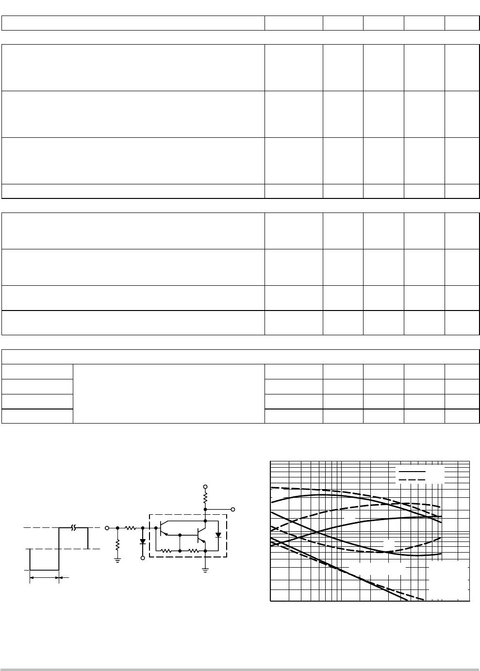
Monolithic Construction with Built−In Base−Emitter Shunt Resistor
Pb−Free Packages are Available*
MAXIMUM RATINGS
Rating Symbol
TIP140
TIP145
TIP141
TIP146
TIP142
TIP147
Unit
Collector − Emitter Voltage V
CEO
60 80 100 Vdc
CollectorBase Voltage V
CB
60 80 100 Vdc
EmitterBase Voltage V
EB
5.0 Vdc
Collector Current
− Continuous
− Peak (Note 1)
I
C
10
15
Adc
Base Current − Continuous I
B
0.5 Adc
Total Power Dissipation
@ T
C
= 25_C
P
D
125 W
Operating and Storage
Junction Temperature Range
T
J
, T
stg
−65 to +150
_C
THERMAL CHARACTERISTICS
Characteristic Symbol Max Unit
Thermal Resistance,
Junction−to−Case
R
q
JC
1.0 °C/W
Thermal Resistance,
Junction−to−Ambient
R
q
JA
35.7 °C/W
Maximum ratings are those values beyond which device damage can occur.
Maximum ratings applied to the device are individual stress limit values (not
normal operating conditions) and are not valid simultaneously. If these limits are
exceeded, device functional operation is not implied, damage may occur and
reliability may be affected.
1. 5 ms, v 10% Duty Cycle.
*For additional information on our Pb−Free strategy and soldering details, please
download the ON Semiconductor Soldering and Mounting Techniques
Reference Manual, SOLDERRM/D.
Preferred devices are recommended choices for future use
and best overall value.
10 AMPERE
DARLINGTON
COMPLEMENTARY SILICON
POWER TRANSISTORS
60−100 VOLTS, 125 WATTS
See detailed ordering and shipping information in the package
dimensions section on page 2 of this data sheet.
ORDERING INFORMATION
http://onsemi.com
SOT−93 (TO−218)
CASE 340D
STYLE 1
MARKING DIAGRAM
A = Assembly Location
Y = Year
WW = Work Week
TIP14x = Device Code
x = 0, 1, 2, 5, 6, or 7
G = Pb−Free Package
AYWWG
TIP14x
TIP140, TIP141, TIP142, (NPN); TIP145, TIP146, TIP147, (PNP)
http://onsemi.com
2
DARLINGTON SCHEMATICS
BASE
EMITTER
COLLECTOR
8.0 k 40
BASE
EMITTER
COLLECTOR
8.0 k 40
NPN
TIP140
TIP141
TIP142
PNP
TIP145
TIP146
TIP147
ORDERING INFORMATION
Device Package Shipping
TIP140 SOT−93 (TO−218) 30 Units / Rail
TIP140G SOT−93 (TO−218)
(Pb−Free)
30 Units / Rail
TIP141 SOT−93 (TO−218) 30 Units / Rail
TIP141G SOT−93 (TO−218)
(Pb−Free)
30 Units / Rail
TIP142 SOT−93 (TO−218) 30 Units / Rail
TIP142G SOT−93 (TO−218)
(Pb−Free)
30 Units / Rail
TIP145 SOT−93 (TO−218) 30 Units / Rail
TIP145G SOT−93 (TO−218)
(Pb−Free)
30 Units / Rail
TIP146 SOT−93 (TO−218) 30 Units / Rail
TIP146G SOT−93 (TO−218)
(Pb−Free)
30 Units / Rail
TIP147 SOT−93 (TO−218) 30 Units / Rail
TIP147G SOT−93 (TO−218)
(Pb−Free)
30 Units / Rail
TIP140, TIP141, TIP142, (NPN); TIP145, TIP146, TIP147, (PNP)
http://onsemi.com
3
ELECTRICAL CHARACTERISTICS (T
C
= 25_C unless otherwise noted)
Characteristic Symbol Min Typ Max Unit
OFF CHARACTERISTICS
Collector−Emitter Sustaining Voltage (Note 2)
(I
C
= 30 mA, I
B
= 0) TIP140, TIP145
TIP141, TIP146
TIP142, TIP147
V
CEO(sus)
60
80
100
Vdc
Collector Cutoff Current
(V
CE
= 30 Vdc, I
B
= 0) TIP140, TIP145
(V
CE
= 40 Vdc, I
B
= 0) TIP141, TIP146
(V
CE
= 50 Vdc, I
B
= 0) TIP142, TIP147
I
CEO
2.0
2.0
2.0
mA
Collector Cutoff Current
(V
CB
= 60 V, I
E
= 0) TIP140, TIP145
(V
CB
= 80 V, I
E
= 0) TIP141, TIP146
(V
CB
= 100 V, I
E
= 0) TIP142, TIP147
I
CBO
1.0
1.0
1.0
mA
Emitter Cutoff Current (V
BE
= 5.0 V) I
EBO
2 0 mA
ON CHARACTERISTICS (Note 2)
DC Current Gain
(I
C
= 5.0 A, V
CE
= 4.0 V)
(I
C
= 10 A, V
CE
= 4.0 V)
h
FE
1000
500
Collector−Emitter Saturation Voltage
(I
C
= 5.0 A, I
B
= 10 mA)
(I
C
= 10 A, I
B
= 40 mA)
V
CE(sat)
2.0
3.0
Vdc
Base−Emitter Saturation Voltage
(I
C
= 10 A, I
B
= 40 mA)
V
BE(sat)
3.5 Vdc
Base−Emitter On Voltage
(I
C
= 10 A, V
CE
= 4.0 Vdc)
V
BE(on)
3.0 Vdc
SWITCHING CHARACTERISTICS
Resistive Load (See Figure 1)
Delay Time
(V
CC
= 30 V, I
C
= 5.0 A,
I
B
= 20 mA, Duty Cycle v 2.0%,
I
B1
= I
B2
, R
C
& R
B
Varied, T
J
= 25_C)
t
d
0.15
ms
Rise Time t
r
0.55
ms
Storage Time t
s
2.5
ms
Fall Time t
f
2.5
ms
2. Pulse Test: Pulse Width = 300 ms, Duty Cycle v 2.0%.
Figure 1. Switching Times Test Circuit
10
0.2
Figure 2. Switching Times
I
C
, COLLECTOR CURRENT (AMP)
t, TIME (s)μ
5.0
2.0
0.5
0.1
0.5 1.0 3.0 5.0 10 20
0.2
PNP
NPN
t
f
t
r
t
s
t
d
@ V
BE(off)
= 0
V
2
approx
+12 V
V
1
appox.
−8.0 V
t
r
, t
f
10 ns
DUTY CYCLE = 1.0%
25 ms
0
R
B
51
D
1
+4.0 V
V
CC
−30 V
R
C
TUT
8.0 k
40
SCOPE
for t
d
and t
r
, D1 is disconnected
and V
2
= 0
R
B
& R
C
VARIED TO OBTAIN DESIRED CURRENT LEVELS
D
1
, MUST BE FAST RECOVERY TYPE, eg:
1N5825 USED ABOVE I
B
100 mA
MSD6100 USED BELOW I
B
100 mA
V
CC
= 30 V
I
C
/I
B
= 250
I
B1
= I
B2
T
J
= 25°C
For NPN test circuit reverse diode and voltage polarities.
1.0

TIP142

Mfr. #:
Manufacturer:
STMicroelectronics
Description:
Darlington Transistors NPN Power Darlington
Lifecycle:
New from this manufacturer.
Delivery:
DHL FedEx Ups TNT EMS
Payment:
T/T Paypal Visa MoneyGram Western Union

Products related to this Datasheet