ISL99201IRTBZ-TK

4
FN6742.2
November 1, 2013
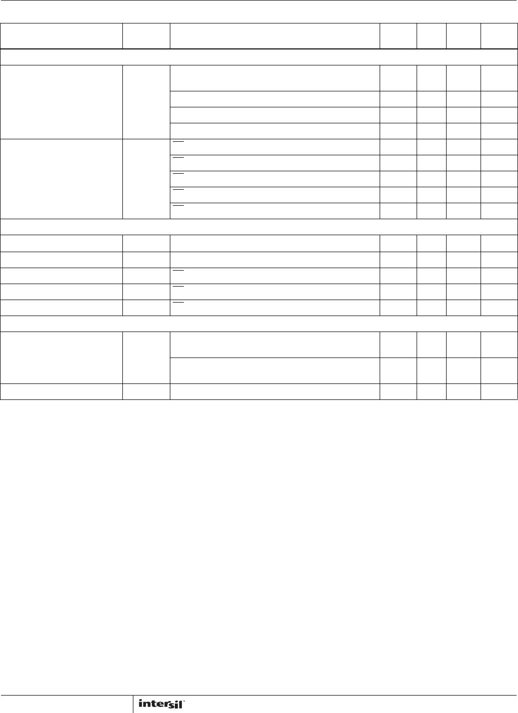
GAIN CONTROL
Closed-Loop Gain D version user program
(Max Gain, Ri = 0)
27.5 28.5 29.5 dB
A version 5.7 6 6.3 dB
B version 9.2 9.6 10 dB
C version 11.5 12 12.5 dB
Differential Input Impedance Z
IN
SD = V
DD
, A version 70 k
SD = V
DD
, B version 46.25 k
SD
= V
DD
, C version 35 k
SD
= V
DD
, D version, Ri = 2.5k 7.5 k
SD = GND 100 k
SHUTDOWN CONTROL
Input Voltage High V
IH
1.2 V
Input Voltage Low V
IL
0.5 V
Turn-on Time t
WU
SD rising edge from GND to V
DD
3.5 ms
Turn-off Time t
SD
SD falling edge from V
DD
to GND 5 µs
Output Impedance Z
OUT
SD = GND >100 k
NOISE PERFORMANCE
Output Voltage Noise E
n
V
DD
= 3.6V, f = 20Hz to 20kHz, inputs are AC grounded,
A
V
= 6dB, A-weighting
27 µV
V
DD
= 3.6V, f = 20Hz to 20kHz, inputs are AC grounded,
A
V0
= 6dB, no weighting
35 µV
Signal-to-Noise Ratio SNR P
OUT
= 1W, R
L
= 8 102 dB
NOTES:
4. Limits established by Characterization and are not production tested
5. Parameters with MIN and/or MAX limits are 100% tested at +25°C, unless otherwise specified. Temperature limits established by characterization
and are not production tested.
Electrical Specifications Typical Values Are Tested at V
DD
= 5V and the Ambient Temperature at +25°C. (Continued)
PARAMETER SYMBOL TEST CONDITIONS
MIN
(Note 5) TYP
MAX
(Note 5) UNITS
ISL99201
5
FN6742.2
November 1, 2013
Pin Descriptions
SD
Shutdown Active Low. This signal is used to shut down and activate
the part. It is 1.8V to 5V compatible. During shutdown, the part
draws less than 100nA input current. Coming out of shutdown takes
3.5ms and going into shutdown is instantaneous.
SYNC
External clock input. This pin allows the chip to be synchronized to a
system clock. This helps in folding the spectral components and the
switching harmonic out of band of interest. The range of SYNC
frequency is from 250kHz to 800kHz.
IN+
Positive Differential Input.
IN-
Negative Differential Input.
V
O
+
Positive BTL output.
GND
Ground.
V
DD
Power Supply.
V
O
-
Negative BTL output.
Block Diagram (Notes)
SAWTOOTH
GENERATOR
SHUTDOWN
LOGIC
OVER
CURRENT
PROTECTION
BIAS AND
REFERENCE
CLICK AND POP
SUPPRESSION
VDD
VO-
VO+
SD
SYNC
1
IN+
IN-
GND
GATE DRIVE
WITH
SRC
GATE DRIVE
WITH
SRC
COMP
COMP
VDD
VDD
+180°
+
-
-
+
-
+
+
-
+
-
Notes:
Gain = 6dB, 9.6dB, 12dB (gain setting)
Gain = ; with external resistor
140k
(Ri + 5kΩ)
ISL99201
6
FN6742.2
November 1, 2013
Typical Performance Characteristics
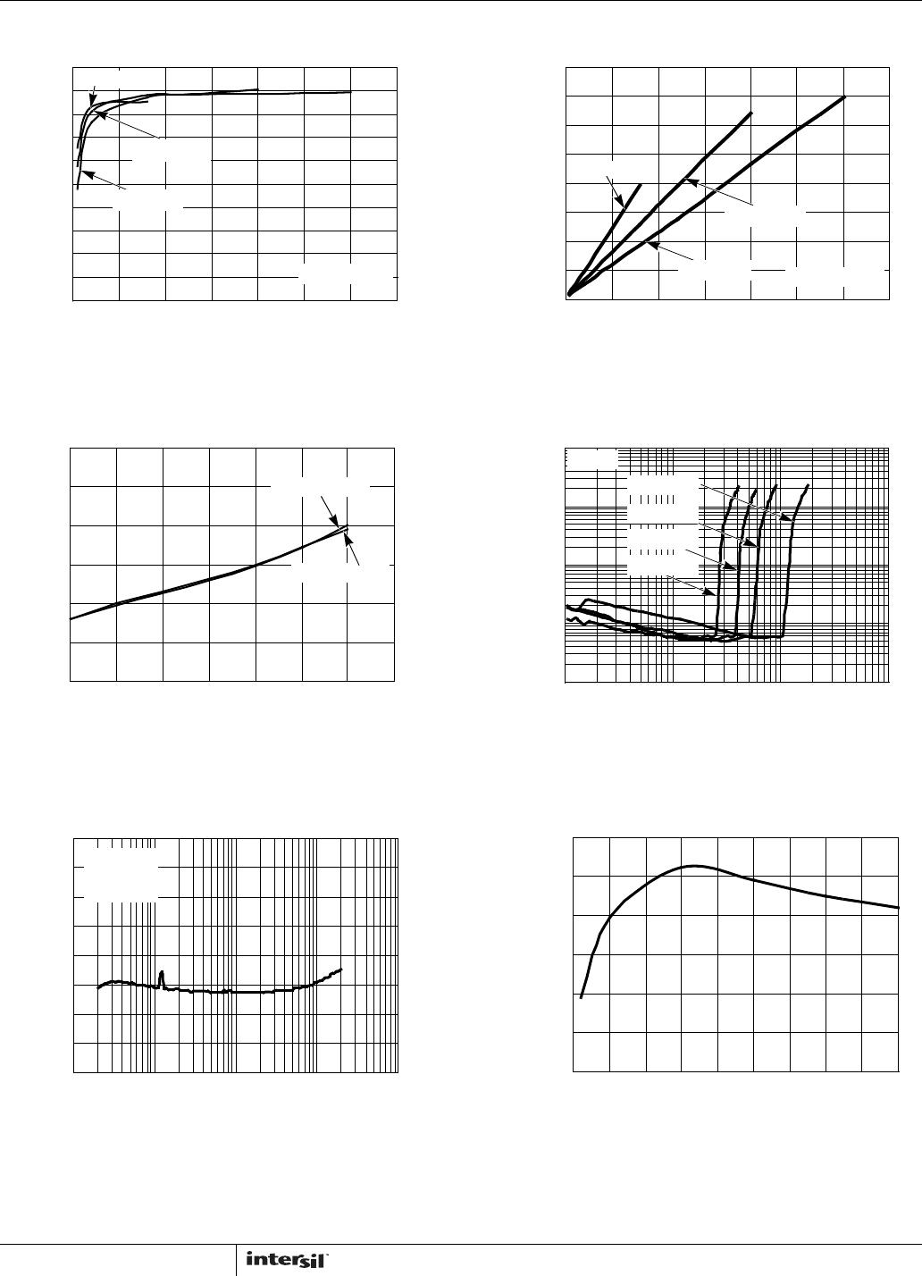
FIGURE 1. EFFICIENCY vs OUTPUT POWER
FIGURE 2. SUPPLY CURRENT vs OUTPUT POWER
FIGURE 3. SUPPLY CURRENT vs SUPPLY VOLTAGE
FIGURE 4. TOTAL HARMONIC DISTORTION + NOISE vs
OUTPUT POWER
FIGURE 5. COMMON MODE REJECTION MODE vs
FREQUENCY
FIGURE 6. POWER DISSIPATION vs OUTPUT POWER
0
10
20
30
40
50
60
70
80
90
100
0 0.250.500.751.001.251.501.75
EFFICIENCY (%)
V
DD
= 2.5 V
V
DD
= 3.6 V
R
L
= 8+ 33µH
OUTPUT POWER (W)
V
DD
= 5 V
0
50
100
150
200
250
300
350
400
0 0.25 0.50 0.75 1.0 1.25 1.50 1.75
OUTPUT POWER (W)
SUPPLY CURRENT (mA)
V
DD
= 2.5 V
V
DD
= 3.6 V
V
DD
= 5 V
R
L
= 8+ 33µH
2.0
2.5
3.0
3.5
4.0
4.5
5.0
2.5 3.0 3.5 4.0 4.5 5.0 5.5 6.0
INPUT SUPPLY (V)
SUPPLY CURRENT (mA)
R
L
= 8+ 33µH
R
L
= NO LOAD
0.01
0.10
1
10
100
0.01 0.10 1 10
TOTAL HARMONIC DISTORTION (%)
V
DD
= 5V
R
L
= 8
V
DD
= 3.6V
V
DD
= 3V
V
DD
= 2.5V
OUTPUT POWER (W)
-100
-90
-80
-70
-60
-50
-40
-30
-20
10 100 1k 10k 100k
FREQUENCY (Hz)
CMRR (COMMON MODE
REJECTION RATIO - dB)
V
DD
= 3.6V
V
IC
= 1V
P-P
R
L
= 8
0
0.05
0.10
0.15
0.20
0.25
0.30
0 0.1 0.2 0.3 0.4 0.5 0.6 0.7 0.8 0.9
OUTPUT POWER (W)
POWER DISSIPATION (W)
ISL99201

ISL99201IRTBZ-TK

Mfr. #:
Manufacturer:
Renesas / Intersil
Description:
Audio Amplifiers FILTER-LESS HI EFF 15W 9DB CLASS D
Lifecycle:
New from this manufacturer.
Delivery:
DHL FedEx Ups TNT EMS
Payment:
T/T Paypal Visa MoneyGram Western Union