BU2506FV,BU2505FV
Technical Note
6/10
www.rohm.com
2011.04 - Rev.B
© 2011ROHM Co., Ltd. All rights reserved.
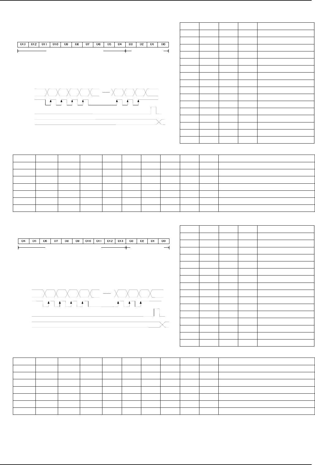
D 0D 1D 2D3 D13D12D 11
DI
CLK
LD
DACOUT
D 4
DDRESS
LSB
DDRESS
MSB
DATA
MSB
DATA
LSB
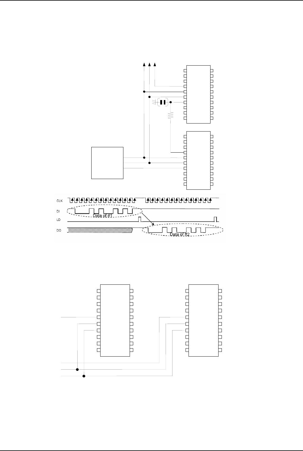
●Command Transmission
1) Reverse = open (or VCC short-circuit) setting
(1) Data format
(2) Data timing diagram
D3 D2 D1 D0 Address Selection
0 0 0 0 Inconsequential
0 0 0 1 AO1 selection
0 0 1 0 AO2 selection
0 0 1 1 AO3 selection
0 1 0 0 AO4 selection
0 1 0 1 AO5 selection
0 1 1 0 AO6 selection
0 1 1 1 AO7 selection
1 0 0 0 AO8 selection
1 0 0 1 AO9 selection
*1
1 0 1 0 AO10 selection
*1
1 0 1 1 Inconsequential
1 1 0 0 Inconsequential
1 1 0 1 Inconsequential
1 1 1 0 Inconsequential
1 1 1 1 Inconsequential
D13 D12 D11 D10 D9 D8 D7 D6 D5 D4 D/A output (VrefH=VDD, VrefL=VSS)
0 0 0 0 0 0 0 0 0 0 VrefL
0 0 0 0 0 0 0 0 0 1 (VrefH-VrefL)/1024×1+VrefL
0 0 0 0 0 0 0 0 1 0 (VrefH-VrefL)/1024×2+VrefL
0 0 0 0 0 0 0 0 1 1 (VrefH-VrefL)/1024×3+VrefL
: : : : : : : : : : :
1 1 1 1 1 1 1 1 1 0 (VrefH-VrefL)/1024×1022+VrefL
1 1 1 1 1 1 1 1 1 1 (VrefH-VrefL)/1024×1023+VrefL
2) Reverse = L setting
(1) Data format
(2) Data timing diagram
D3 D2 D1 D0 Address selection
0 0 0 0 Inconsequential
0 0 0 1 AO1 selection
0 0 1 0 AO2 selection
0 0 1 1 AO3 selection
0 1 0 0 AO4 selection
0 1 0 1 AO5 selection
0 1 1 0 AO6 selection
0 1 1 1 AO7 selection
1 0 0 0 AO8 selection
1 0 0 1 AO9 selection
*1
1 0 1 0 AO10 selection
*1
1 0 1 1 Inconsequential
1 1 0 0 Inconsequential
1 1 0 1 Inconsequential
1 1 1 0 Inconsequential
1 1 1 1 Inconsequential
D4 D5 D6 D7 D8 D9 D10 D11 D12 D13 D/A output (VrefH=VDD, VrefL=VSS)
0 0 0 0 0 0 0 0 0 0 VrefL
1 0 0 0 0 0 0 0 0 0 (VrefH-VrefL)/1024×1+VrefL
0 1 0 0 0 0 0 0 0 0 (VrefH-VrefL)/1024×2+VrefL
1 1 0 0 0 0 0 0 0 0 (VrefH-VrefL)/1024×3+VrefL
: : : : : : : : : : :
0 1 1 1 1 1 1 1 1 1 (VrefH-VrefL)/1024×1022+VrefL
1 1 1 1 1 1 1 1 1 1 (VrefH-VrefL)/1024×1023+VrefL
*1 In the BU2506FV, this channel is for testing, therefore, do not designate.
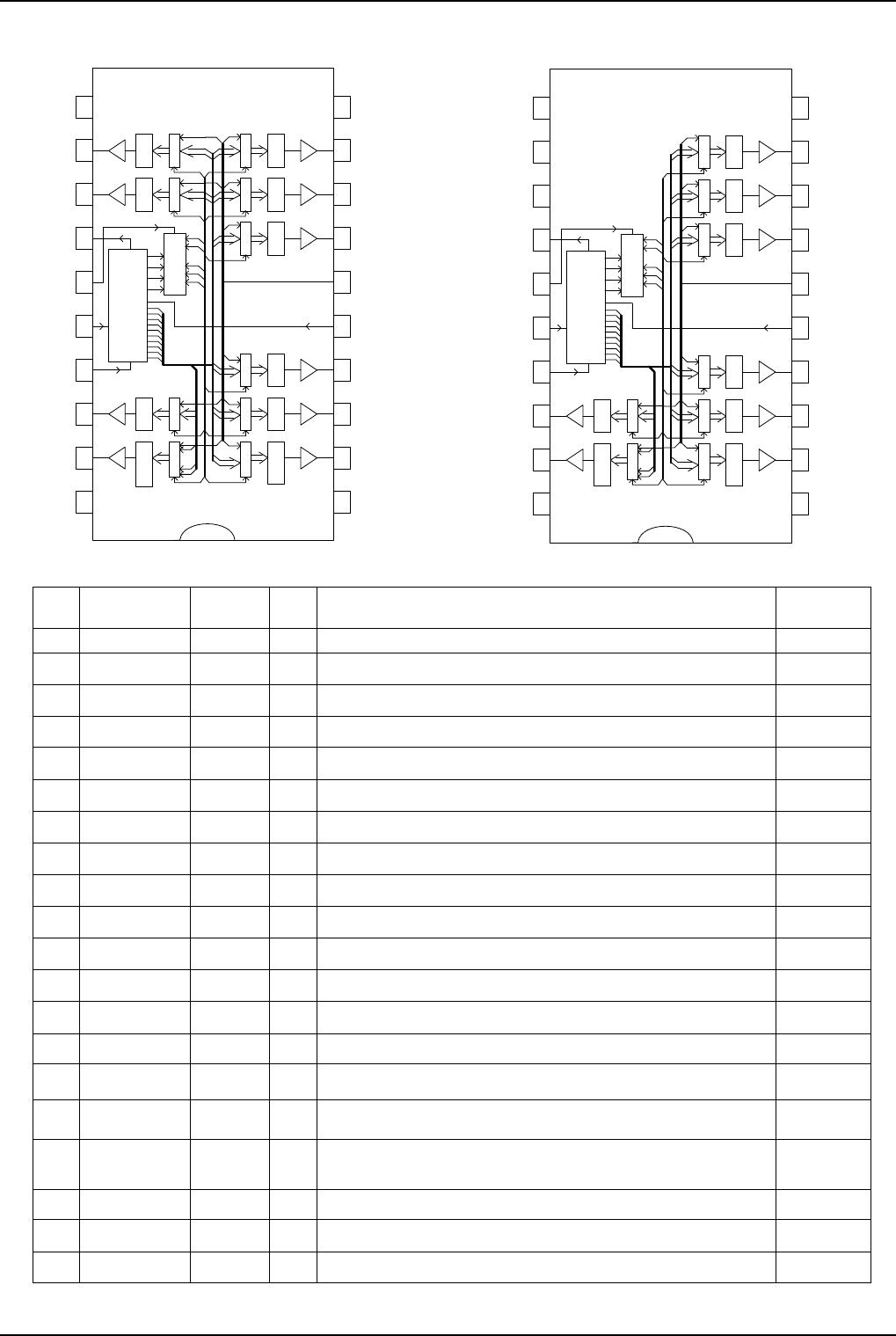
For D/A converter output setting
For address selection
For D/A converter output setting
For address selection
D 0D1D 2D3 D4D5D 6
DI
CLK
LD
DACOUT
D13
DATA
MSB
DATA
LSB
DDRESS
LSB
DDRESS
MSB