3
COMMERCIAL, INDUSTRIAL AND MILITARY
TEMPERATURE RANGES
IDT7203/7204/7205/7206/7207/7208 CMOS ASYNCHRONOUS FIFO
2,048 x 9, 4,096 x 9, 8,192 x 9, 16,384 x 9, 32,768 x 9 and 65,536 x 9
IDT7203
(1)
IDT7203
IDT7204
(1)
IDT7204
Commercial and Industrial Military
(3)
tA = 12, 15, 20, 25, 35, 50 ns tA = 20, 30, 40 ns
Symbol Parameter Min. Typ. Max. Min. Typ. Max. Unit
ILI
(6)
Input Leakage Current (Any Input) –1 — 1 –1 — 1 μA
ILO
(7)
Output Leakage Current –10 — 10 –10 — 10 μA
VOH Output Logic “1” Voltage IOH = –2mA 2.4 — — 2.4 — — V
VOL Output Logic “0” Voltage IOL = 8mA — — 0.4 — — 0.4 V
ICC1
(8,9,10)
Active Power Supply Current — — 120 — — 150 mA
ICC2
(8,10,11)
Standby Current (R=W=RS=FL/RT=VIH) ——12— —25mA
ICC3
(8,10,12)
Power Down Current — — 2 — — 4 mA
AC TEST CONDITIONS
NOTES:
1. Industrial temperature range product for 15ns and 25ns speed grades are available
as a standard device.
2. Industrial temperature range product for 25ns speed grade only is available as a standard
device. All other speed grades are available by special order.
3. Military temperature range product for the 40ns is only available for 7203.
4. Commercial temperature range product for the 12ns not available.
5. Commercial temperature range product for the 12ns, 15ns and 50ns not available.
IDT7205
(1)
IDT7205
IDT7206
(2,4)
IDT7206
IDT7207
(2,4)
IDT7207
IDT7208
(2,5)
Commercial and Industrial Military
tA = 12, 15, 20, 25, 35, 50 ns tA = 20, 30 ns
Symbol Parameter Min. Typ. Max. Min. Typ. Max. Unit
ILI
(6)
Input Leakage Current (Any Input) –1 — 1 –1 — 1 μA
ILO
(7)
Output Leakage Current –10 — 10 –10 — 10 μA
VOH Output Logic “1” Voltage IOH = –2mA 2.4 — — 2.4 — — V
VOL Output Logic “0” Voltage IOL = 8mA — — 0.4 — — 0.4 V
ICC1
(8,9,10)
Active Power Supply Current — — 120 — — 150 mA
ICC2
(8,10,11)
Standby Current (RS=FL/RT=VIH)——12——25mA
I
CC3
(8,10,12)
Power Down Current — — 8 — — 12 mA
Input Pulse Levels GND to 3.0V
Input Rise/Fall Times 5ns
Input Timing Reference Levels 1.5V
Output Reference Levels 1.5V
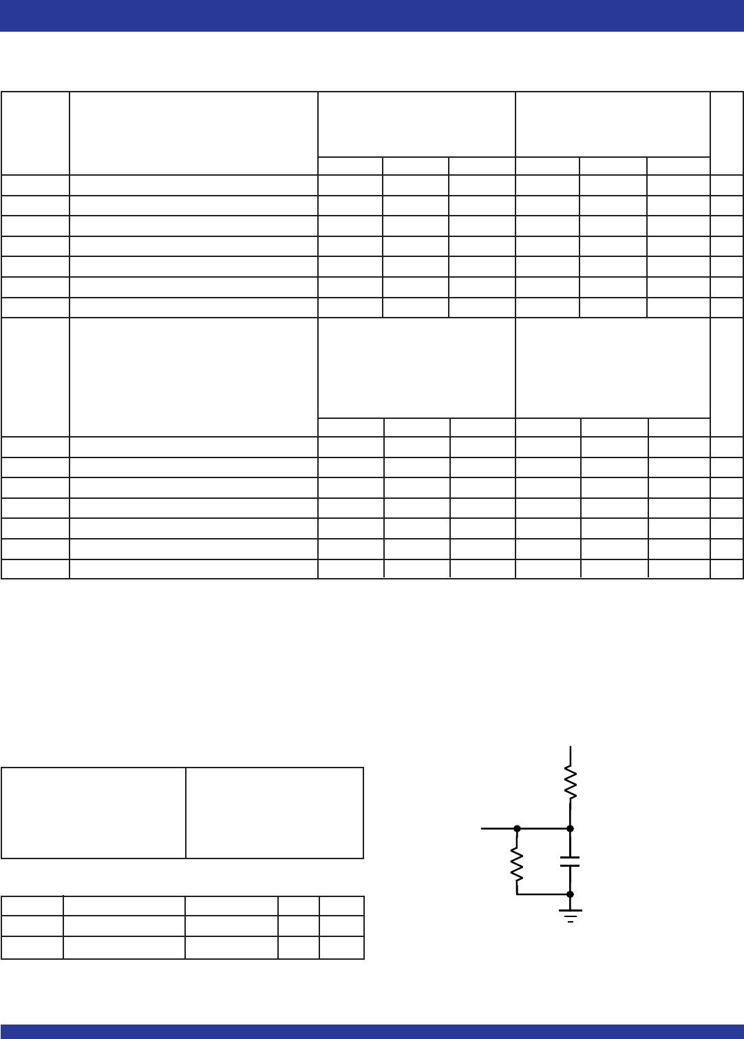
Output Load See Figure 1
1.1KΩ
30pF*
680Ω
5V
D.U.T.
or equivalent circuit
2661 drw03
DC ELECTRICAL CHARACTERISTICS
(Commercial: VCC = 5V ± 10%, TA = 0°C to +70°C; Industrial: VCC = 5V ± 10%, TA = –40°C to +85°C; Military: VCC = 5V ± 10%, TA = –55°C to +125°C)
6. Measurements with 0.4 ≤ VIN ≤ VCC.
7. R ≥ VIH, 0.4 ≤ VOUT ≤ VCC.
8. Tested with outputs open (IOUT = 0).
9. R and W toggle at 20 MHz and data inputs switch at 10 MHz.
10. ICC measurements are made with outputs open.
11. All Inputs = VCC - 0.2V or GND + 0.2V, except R and W, which toggle at 20MHz.
12. All Inputs = VCC - 0.2V or GND + 0.2V, except R and W = VCC -0.2V.
CAPACITANCE
(1)
(TA = +25°C, f = 1.0 MHz)
NOTES:
1. This parameter is sampled and not 100% tested.
2. With output deselected.
Symbol Parameter Condition Max. Unit
CIN
(1)
Input Capacitance VIN = 0V 10 pF
C
OUT
(1,2)
Output Capacitance VOUT = 0V 10 pF
Figure 1. Output Load
*Includes jig and scope capacitances.