PZT2222AT1G

© Semiconductor Components Industries, LLC, 2013
August, 2013 Rev. 9
1 Publication Order Number:
PZT2222AT1/D
PZT2222A
NPN Silicon Planar
Epitaxial Transistor
This NPN Silicon Epitaxial transistor is designed for use in linear
and switching applications. The device is housed in the SOT223
package which is designed for medium power surface mount
applications.
Features
PNP Complement is PZT2907AT1
The SOT223 Package Can be Soldered Using Wave or Reflow
SOT223 Package Ensures Level Mounting, Resulting in Improved
Thermal Conduction, and Allows Visual Inspection of Soldered
Joints
The Formed Leads Absorb Thermal Stress During Soldering,
Eliminating the Possibility of Damage to the Die
Available in 12 mm Tape and Reel
S Prefix for Automotive and Other Applications Requiring Unique
Site and Control Change Requirements; AECQ101 Qualified and
PPAP Capable
These Devices are PbFree, Halogen Free/BFR Free and are RoHS
Compliant*
MAXIMUM RATINGS
Rating Symbol Value Unit
CollectorEmitter Voltage V
CEO
40 Vdc
CollectorBase Voltage V
CBO
75 Vdc
EmitterBase Voltage
(Open Collector)
V
EBO
6.0 Vdc
Collector Current I
C
600 mAdc
Total Power Dissipation
up to T
A
= 25°C (Note 1)
P
D
1.5
W
Storage Temperature Range° T
stg
65 to +150 °C
Junction Temperature° T
J
150 °C
Stresses exceeding Maximum Ratings may damage the device. Maximum
Ratings are stress ratings only. Functional operation above the Recommended
Operating Conditions is not implied. Extended exposure to stresses above the
Recommended Operating Conditions may affect device reliability.
1. Device mounted on an epoxy printed circuit board 1.575 inches x 1.575 inches x
0.059 inches; mounting pad for the collector lead min. 0.93 inches
2
.
THERMAL CHARACTERISTICS
Rating Symbol Value Unit
Thermal Resistance,
JunctiontoAmbient
R
q
JA
83.3 °C/W
Lead Temperature for Soldering,
0.0625 from case
Time in Solder Bath
T
L
260
10
°C
Sec
*For additional information on our PbFree strategy and soldering details, please download the ON Semiconductor Soldering and Mounting
Techniques Reference Manual, SOLDERRM/D.
http://onsemi.com
MARKING DIAGRAM
SOT223 (TO261)
CASE 318E04
STYLE 1
Device Package Shipping
ORDERING INFORMATION
PZT2222AT1G SOT223
(PbFree)
1,000 Tape & Reel
For information on tape and reel specifications,
including part orientation and tape sizes, please
refer to our Tape and Reel Packaging Specifications
Brochure, BRD8011/D.
A = Assembly Location
Y = Year
M = Month Code
G = PbFree Package
BASE
1
COLLECTOR
2, 4
3
EMITTER
SOT223 PACKAGE
NPN SILICON TRANSISTOR
SURFACE MOUNT
PZT2222AT3G SOT223
(PbFree)
4,000 Tape & Reel
AYM
P1FG
G
(Note: Microdot may be in either location)
SPZT2222AT1G SOT223
(PbFree)
1,000 Tape & Reel
1
2
3
4
PZT2222A
http://onsemi.com
2
ELECTRICAL CHARACTERISTICS (T
A
= 25°C unless otherwise noted)
Characteristic
Symbol Min Max Unit
OFF CHARACTERISTICS
CollectorEmitter Breakdown Voltage (I
C
= 10 mAdc, I
B
= 0) V
(BR)CEO
40 Vdc
CollectorBase Breakdown Voltage (I
C
= 10 mAdc, I
E
= 0)
V
(BR)CBO
°75° Vdc
EmitterBase Breakdown Voltage (I
E
= 10 mAdc, I
C
= 0)
V
(BR)EBO
6.0 Vdc
BaseEmitter Cutoff Current (V
CE
= 60 Vdc, V
BE
= 3.0 Vdc) I
BEX
20 nAdc
CollectorEmitter Cutoff Current (V
CE
= 60 Vdc, V
BE
= 3.0 Vdc) I
CEX
10 nAdc
EmitterBase Cutoff Current (V
EB
= 3.0 Vdc, I
C
= 0) I
EBO
100 nAdc
CollectorBase Cutoff Current
(V
CB
= 60 Vdc, I
E
= 0)
(V
CB
= 60 Vdc, I
E
= 0, T
A
= 125°C)
I
CBO
10
10
nAdc
mAdc
ON CHARACTERISTICS
DC Current Gain
(I
C
= 0.1 mAdc, V
CE
= 10 Vdc)
(I
C
= 1.0 mAdc, V
CE
= 10 Vdc)
(I
C
= 10 mAdc, V
CE
= 10 Vdc)
(I
C
= 10 mAdc, V
CE
= 10 Vdc, T
A
= 55°C)
(I
C
= 150 mAdc, V
CE
= 10 Vdc)
(I
C
= 150 mAdc, V
CE
= 1.0 Vdc)
(I
C
= 500 mAdc, V
CE
= 10 Vdc)
h
FE
35
50
70
35
100
50
40
300
CollectorEmitter Saturation Voltages
(I
C
= 150 mAdc, I
B
= 15 mAdc)
(I
C
= 500 mAdc, I
B
= 50 mAdc)
V
CE(sat)
0.3
1.0
Vdc
BaseEmitter Saturation Voltages
(I
C
= 150 mAdc, I
B
= 15 mAdc)
(I
C
= 500 mAdc, I
B
= 50 mAdc)
V
BE(sat)
0.6
1.2
2.0
Vdc
Input Impedance°
(V
CE
= 10 Vdc, I
C
= 1.0 mAdc, f = 1.0 kHz)
(V
CE
= 10 Vdc, I
C
= 10 mAdc, f = 1.0 kHz)
°h
ie
°
2.0
0.25
8.0
1.25
kW
Voltage Feedback Ratio
(V
CE
= 10 Vdc, I
C
= 1.0 mAdc, f = 1.0 kHz)
(V
CE
= 10 Vdc, I
C
= 10 mAdc, f = 1.0 kHz)
h
re
8.0x10
4
4.0x10
4
SmallSignal Current Gain
(V
CE
= 10 Vdc, I
C
= 1.0 mAdc, f = 1.0 kHz)
(V
CE
= 10 Vdc, I
C
= 10 mAdc, f = 1.0 kHz)
ťh
fe
ť
50
75
300
375
Output Admittance°
(V
CE
= 10 Vdc, I
C
= 1.0 mAdc, f = 1.0 kHz)
(V
CE
= 10 Vdc, I
C
= 10 mAdc, f = 1.0 kHz)
°h
oe
°
5.0
25
35
200
mmhos
Noise Figure (V
CE
= 10 Vdc, I
C
= 100 mAdc, f = 1.0 kHz)
F 4.0 dB
DYNAMIC CHARACTERISTICS
CurrentGain Bandwidth Product
(I
C
= 20 mAdc, V
CE
= 20 Vdc, f = 100 MHz)
f
T
300
MHz
Output Capacitance (V
CB
= 10 Vdc, I
E
= 0, f = 1.0 MHz) C
c
8.0 pF
Input Capacitance (V
EB
= 0.5 Vdc, I
C
= 0, f = 1.0 MHz) C
e
25 pF
SWITCHING TIMES (T
A
= 25°C)
Delay Time
(V
CC
= 30 Vdc, I
C
= 150 mAdc,
I
B(on)
= 15 mAdc, V
EB(off)
= 0.5 Vdc)
Figure 1
t
d
10 ns
Rise Time t
r
25
Storage Time
(V
CC
= 30 Vdc, I
C
= 150 mAdc,
I
B(on)
= I
B(off)
= 15 mAdc)
Figure 2
t
s
225 ns
Fall Time t
f
60
PZT2222A
http://onsemi.com
3
V
i
90%
10%
t
p
t
r
0
V
CC
R2
R1
V
i
D.U.T.
V
o
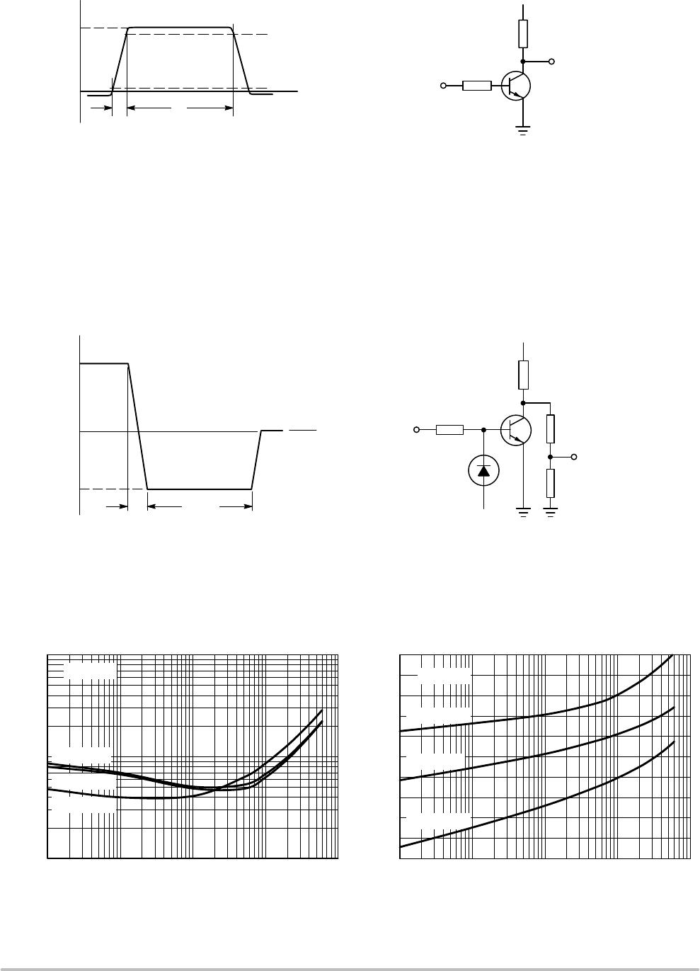
Figure 1. Input Waveform and Test Circuit for Determining Delay Time and Rise Time
Figure 2. Input Waveform and Test Circuit for Determining Storage Time and Fall Time
V
i
= 0.5 V to +9.9 V, V
CC
= +30 V, R1 = 619 W, R2 = 200 W.
PULSE GENERATOR: OSCILLOSCOPE:
PULSE DURATION t
p
3 200 ns INPUT IMPEDANCE Z
i
> 100 kW
RISE TIME t
r
3 2 ns INPUT CAPACITANCE C
i
< 12 pF
DUTY FACTOR d = 0.02 RISE TIME t
r
< 5 ns
t
f
100 ms
-13.8 V
0
+16.2 V
V
i
TIME
V
CC
Vo
OSCILLOSCOPE
D.U.T.
V
i
R2
R3
R4
D1
R1
V
BB
TYPICAL CHARACTERISTICS
Figure 3. Collector Emitter Saturation Voltage
vs. Collector Current
Figure 4. Base Emitter Saturation Voltage vs.
Collector Current
I
C
, COLLECTOR CURRENT (mA) I
C
, COLLECTOR CURRENT (mA)
10001001010.1
0.01
0.1
1
10001001010.1
0.2
0.3
0.5
0.6
0.8
0.9
1.1
1.2
V
CE
, COLLECTOREMITTER
SATURATION VOLTAGE (V)
V
BE(sat)
, BASEEMITTER
SATURATION VOLTAGE (V)
T
A
= 25°C
T
A
= 55°C
T
A
= 150°C
I
C
/I
B
= 10
0.4
0.7
1.0
T
A
= 25°C
T
A
= 55°C
T
A
= 150°C
I
C
/I
B
= 10

PZT2222AT1G

Mfr. #:
Manufacturer:
ON Semiconductor
Description:
Bipolar Transistors - BJT 600mA 75V NPN
Lifecycle:
New from this manufacturer.
Delivery:
DHL FedEx Ups TNT EMS
Payment:
T/T Paypal Visa MoneyGram Western Union

Products related to this Datasheet