8-OUTPUT 1.8V PCIE GEN1-3 ZERO-DELAY/FAN-OUT BUFFER W/ZO=100OHMS 8 APRIL 28, 2016
9DBV0841 DATASHEET
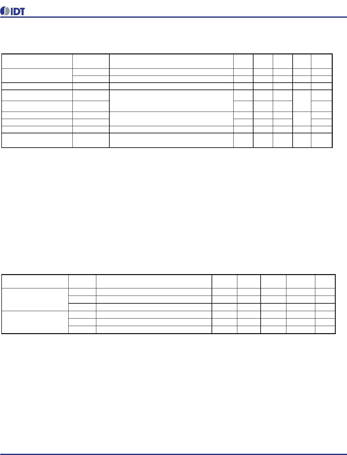
Electrical Characteristics–Output Duty Cycle, Jitter, Skew and PLL Characteristics
Electrical Characteristics–Phase Jitter Parameters
TA = T
AMB,
Supply Voltages per normal operation conditions, See Test Loads for Loading Conditions
PARAMETER SYMBOL CONDITIONS MIN TYP MAX UNITS NOTES
-3dB point in Hi
h BW Mode 2 2.7 4 MHz 1,5
-3dB point in Low BW Mode 1 1.4 2 MHz 1,5
JPEAK
Peak Pass band Gain 1.1 2 dB 1
Duty Cycle t
D
Measured differentially, PLL Mode 45 50.1 55 % 1
Duty Cycle Distortion t
DCD
Measured differentially, Bypass Mode @100MHz -1 0.03 1 % 1,3
t
dBYP
= 50% 2800 3625 4500 ps 1
t
dPLL
= 50% -100 -4 100 ps 1,4
Skew, Output to Output t
sk3
PLL mode 14 50 ps 1,2
Additive Jitter in Bypass Mode 0.10 25 ps 1,2
1
Guaranteed by desi
n and characterization, not 100% tested in production.
Measured from differential waveform
3
Duty cycle distortion is the difference in duty cycle between the output and the input clock when the device is operated in bypass mode.
4
All outputs at default slew rate
5
The MIN/TYP/MAX values of each BW settin
track each other, i.e., Low BW MAX will never occur with Hi BW MIN.
PLL Bandwidth BW
Skew, Input to Output
Jitter, Cycle to cycle t
jcyc-cyc
TA = T
AMB,
Supply Voltages per normal operation conditions, See Test Loads for Loading Conditions
PARAMETER SYMBOL CONDITIONS MIN TYP MAX
INDUSTRY
LIMIT UNITS Notes
t
jphPCIeG1
PCIe Gen 1 24 32 86 ps (p-p)
1,2,3,
5
10kHz < f < 1.5MHz
(rms)
5
PCIe Gen 2 High Band
1.5MHz < f < Nyquist (50MHz)
1.7 2.3
3.1
ps
(rms)
1,2,3,
5
t
jphPCIeG3
PCIe Gen 3
(PLL BW of 2-4 or 2-5MHz, CDR = 10MHz)
0.4 0.6
1
ps
(rms)
1,2,3,
5
t
jphSGMII
125MHz, 1.5MHz to 10MHz, -20dB/decade
rollover < 1.5MHz, -40db/decade rolloff > 10MHz
2.0 NA
ps
(rms)
1,6
t
jphPCIeG1
PCIe Gen 1 0.6 2.6 N/A ps (p-p)
1,2,3,
5
PCIe Gen 2 Lo Band
10kHz < f < 1.5MHz
0.1 0.3 N/A
ps
(rms)
1,2,3,
4,5
PCIe Gen 2 High Band
1.5MHz < f < Nyquist (50MHz)
(rms)
4
(PLL BW of 2-4 or 2-5MHz, CDR = 10MHz)
(rms)
4
t
jphSGMII
125MHz, 1.5MHz to 10MHz, -20dB/decade
rollover < 1.5MHz, -40db/decade rolloff > 10MHz
0.27 N/A
ps
(rms)
1,6
1
Guaranteed by design and characterization, not 100% tested in production.
4
For RMS figures, additive jitter is calculated by solving the following equation: Additive jitter = SQRT[(total jitter)^2 - (input jitter)^2]
5
Driven by 9FGV0841/9FGL0841 or equivalent
6
Driven by Rohde&Schartz SMA100
Phase Jitter, PLL Mode
t
jphPCIeG2
Additive Phase Jitter,
Bypass Mode
t
jphPCIeG2
2
See http://www.pcisig.com for complete specs
3
Sample size of at least 100K cycles. This figures extrapolates to 108ps pk-pk @ 1M cycles for a BER of 1-12.