© Semiconductor Components Industries, LLC, 2017
March, 2018 Rev. 0
1 Publication Order Number:
NSFV4015SG4/D
NSVF4015SG4
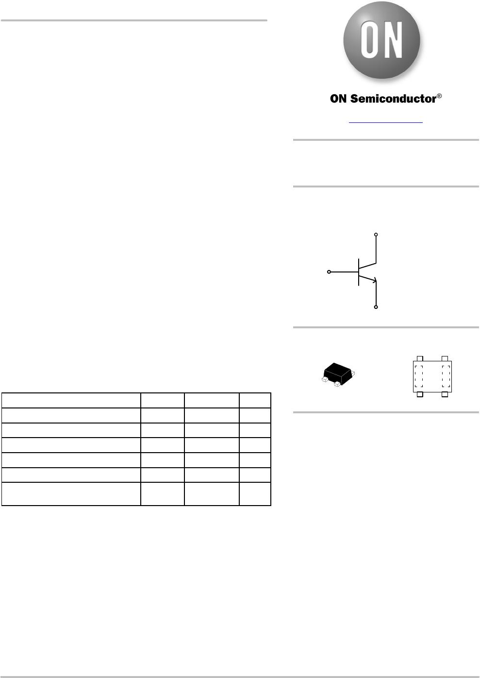
RF Transistor for Low Noise
Amplifier
12 V, 100 mA, f
T
= 10 GHz typ.
This RF transistor is designed for low noise amplifier applications.
MCPH package is suitable for use under high temperature
environment because it has superior heat radiation characteristics.
This RF transistor is AECQ101 qualified and PPAP capable for
automotive applications.
Features
Lownoise Use: NF = 1.2 dB typ. (f = 1 GHz)
High Cutoff Frequency: f
T
= 10 GHz typ. (V
CE
= 5 V)
High Gain: |S21e|
2
= 17 dB typ. (f = 1 GHz)
MCPH4 Package is Pincompatible with SC82FL
AECQ101 Qualified and PPAP Capable
PbFree, Halogen Free and RoHS Compliance
Typical Applications
Low Noise Amplifier for Digital Radio
Low Noise Amplifier for TV
Low Noise Amplifier for FM Radio
RF Amplifier for UHF Application
Specifications
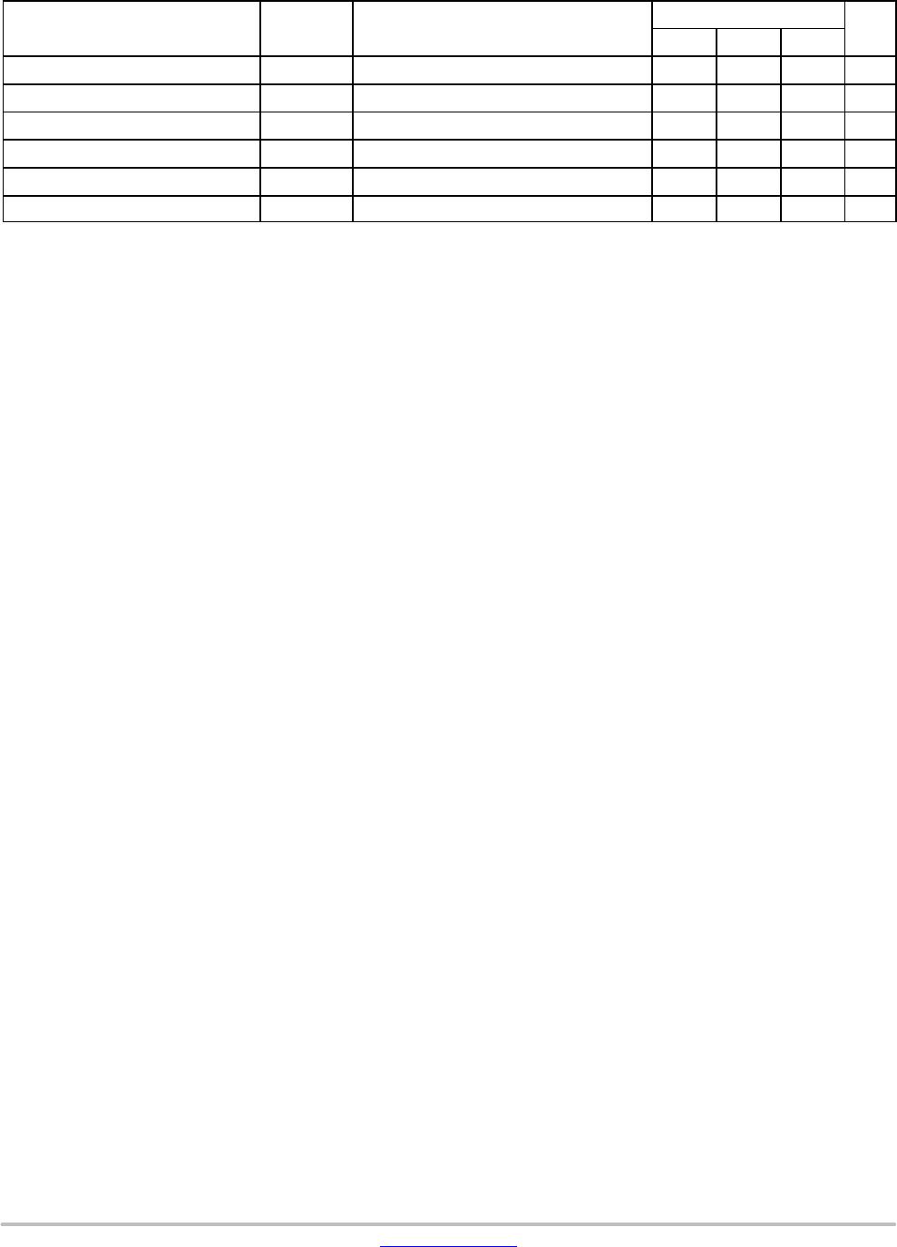
ABSOLUTE MAXIMUM RATINGS
at T
A
= 25°C
Rating Symbol Value Unit
Collector to Base Voltage V
CBO
20 V
Collector to Emitter Voltage V
CEO
12 V
Emitter to Base Voltage V
EBO
2 V
Collector Current I
C
100 mA
Collector Dissipation P
C
450 mW
Operating Junction and Storage
Temperature
T
J
, T
stg
55 to +150 °C
Stresses exceeding those listed in the Maximum Ratings table may damage the
device. If any of these limits are exceeded, device functionality should not be
assumed, damage may occur and reliability may be affected.
www.onsemi.com
MARKING DIAGRAM
ORDERING INFORMATION
ELECTRICAL CONNECTION
NPN
3
2, 4
1
1: Collector
2: Emitter
3: Base
4: Emitter
GN
LOT No.
LOT No.
See detailed ordering and shipping
information on page 10 of this data sheet.
MCPH4
12 V, 100 mA
f
T
= 10 Ghz typ.
RF Transistor
3
4
2
1
NSVF4015SG4
www.onsemi.com
2
Table 1. ELECTRICAL CHARACTERISTICS at T
A
= 25°C (Note 1)
Parameter
Symbol Conditions
Value
Unit
Min Typ Max
Collector Cutoff Current I
CBO
V
CB
= 5 V, I
E
= 0 A
1.0
mA
Emitter Cutoff Current I
EBO
V
EB
= 1 V, I
C
= 0 A
1.0
mA
DC Current Gain h
FE
V
CE
= 5 V, I
C
= 50 mA 60
150
GainBandwidth Product f
T
V
CE
= 5 V, I
C
= 30 mA
8
10
GHz
Forward Transfer Gain | S21e |
2
V
CE
= 5 V, I
C
= 30 mA, f = 1 GHz
14 17 dB
Noise Figure NF
V
CE
= 5 V, I
C
= 10 mA, f = 1 GHz
1.2 1.8 dB
Product parametric performance is indicated in the Electrical Characteristics for the listed test conditions, unless otherwise noted. Product
performance may not be indicated by the Electrical Characteristics if operated under different conditions.
1. Pay attention to handling since it is liable to be affected by static electricity due to the highfrequency process adopted.
NSVF4015SG4
www.onsemi.com
3
TYPICAL CHARACTERISTICS
0 0.2 0.4 0.6 0.8 1.0
012108462
0
10
30
50
100
70
20
40
60
80
90
0
20
10
30
40
60
90
80
70
50
100
2
3
5
7
2
3
5
7
100
10
1000
3257
1.0 10
3257
100
7
2
5
3
7
2
5
3
1.0
0.1
10
325
1000.1
73257
1.0
3257
10
7
2
3
5
7
2
3
5
100
10
1.0
1.0
23 57
10
23 57
100
5
7
2
3
1.0
0.1
Figure 1. I
C
vs. V
CE
Figure 2. I
C
vs. V
BE
Figure 3. h
FE
vs. I
C
Figure 4. C
ob
vs. V
CB
Figure 5. Cre vs. V
CB
Figure 6. f
T
vs. I
C
CollectortoEmitter Voltage, V
CE
V BasetoEmitter Voltage, V
BE
V
Collector Currant, I
C
mA CollectortoBase Voltage, V
BE
V
CollectortoBase Voltage, V
CB
V Collector Current, I
C
mA
Collector Current, I
C
mA
Collector Current, I
c
mA
DC Current Gain, h
FE
Output Capacitance, Cob pF
Reverse Transfer Capacitance, Cre pF
GainBandwidth Product, f
T
GHz
V
CE
= 5 V
I
B
= 0 mA
100 mA
200 mA
300 mA
400 mA
500 mA
600 mA
700 mA
800 mA
900 mA
1000 mA
V
CE
= 5 V
f = 1 MHz
f = 1 MHz
325
1000.1
73257
1.0
3257
10
V
CE
= 5 V
f = 1 GHz

NSVF4015SG4T1G

Mfr. #:
Manufacturer:
ON Semiconductor
Description:
RF Bipolar Transistors BIP NPN 100MA 12V FT=10G
Lifecycle:
New from this manufacturer.
Delivery:
DHL FedEx Ups TNT EMS
Payment:
T/T Paypal Visa MoneyGram Western Union

Products related to this Datasheet