SMB10J22A-M3/5B

SMB10(8)J5.0(C)A thru SMB10(8)J40(C)A
www.vishay.com
Vishay General Semiconductor
Revision: 16-Feb-16
1
Document Number: 89424
For technical questions within your region: DiodesAmericas@vishay.com
, DiodesAsia@vishay.com, DiodesEurope@vishay.com
THIS DOCUMENT IS SUBJECT TO CHANGE WITHOUT NOTICE. THE PRODUCTS DESCRIBED HEREIN AND THIS DOCUMENT
ARE SUBJECT TO SPECIFIC DISCLAIMERS, SET FORTH AT www.vishay.com/doc?91000
High Power Density Surface Mount TRANSZORB
®
Transient Voltage Suppressors
FEATURES
Low profile package
Ideal for automated placement
Glass passivated pellet chip junction
Available in uni-directional and bi-directional
Excellent clamping capability
Very fast response time
Low incremental surge resistance
Meets MSL level 1, per J-STD-020, LF maximum peak
of 260 °C
Material categorization: for definitions of compliance
please see www.vishay.com/doc?99912
TYPICAL APPLCIATIONS
Use in sensitive electronics protection against voltage
transients induced by inductive load switching and lighting
on ICs, MOSFET, signal lines of sensor units for consumer,
computer, industrial, and telecommunication.
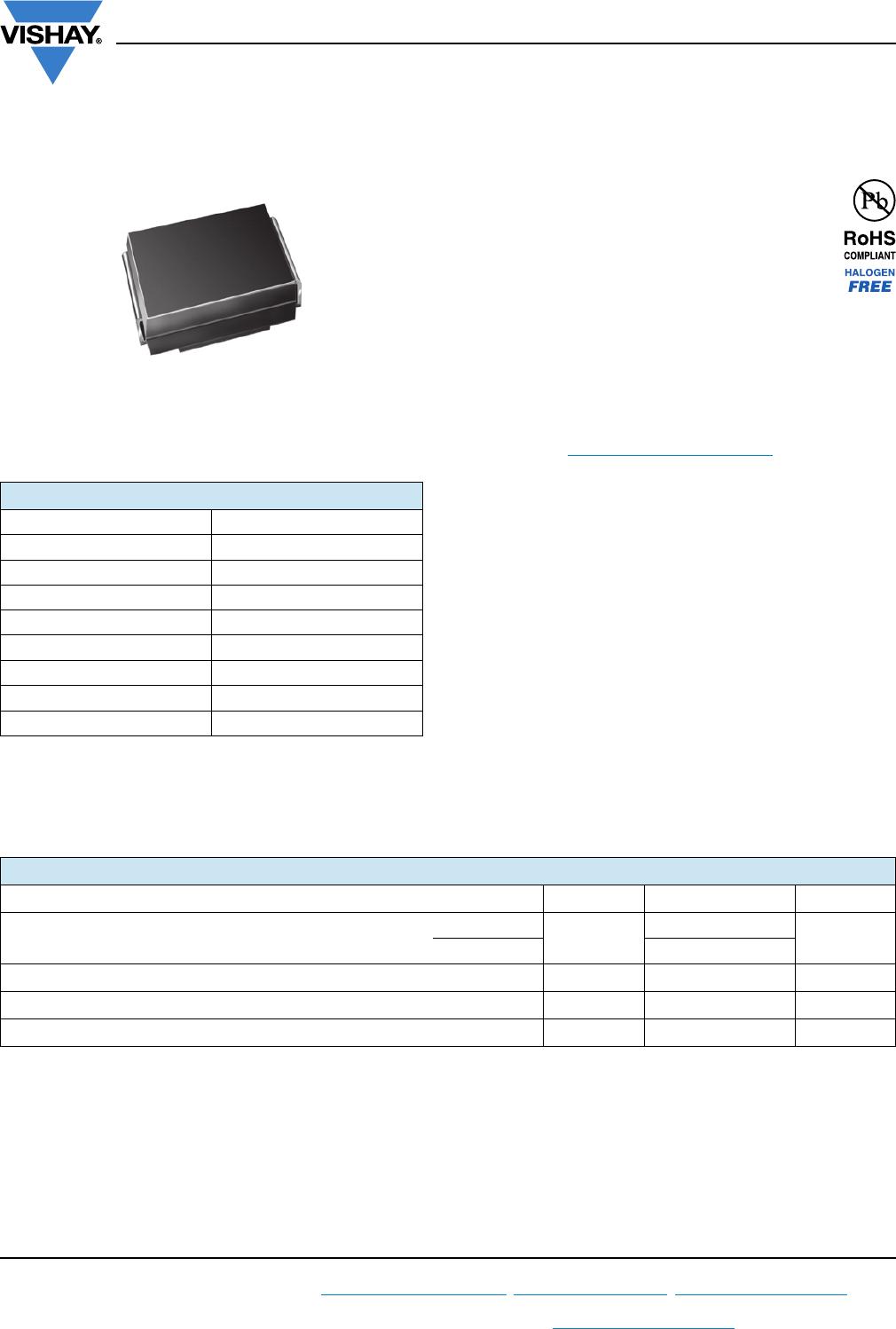
MECHANICAL DATA
Case: DO-214AA (SMB J-Bend)
Molding compound meets UL 94 V-0 flammability rating
Base P/N-M3 - halogen-free, RoHS-compliant, and
commercial grade
Terminals: Matte tin plated leads, solderable per
J-STD-002 and JESD22-B102
M3 suffix meets JESD 201 class 2 whisker test
Polarity: For uni-directional types the color band denotes
cathode end, no marking on bi-directional types
Notes
(1)
Non-repetitive current pulse, per fig. 3 and derated above T
A
= 25 °C per fig. 2.
(2)
Mounted on 0.2" x 0.2" (5.0 mm x 5.0 mm) copper pads to each terminal
PRIMARY CHARACTERISTICS
V
BR
(uni-directional) 6.4 V to 49.1 V
V
BR
(bi-directional) 6.4 V to 49.1 V
V
WM
5.0 V to 40 V
P
PPM
(uni-directional) 1000 W
P
PPM
(bi-directional) 800 W
I
FSM
(uni-directional only) 100 A
T
J
max. 150 °C
Polarity Uni-directional, bi-directional
Package DO-214AA (SMB J-Bend)
DO-214AA (SMB J-Bend)
MAXIMUM RATINGS (T
A
= 25 °C, unless otherwise noted)
PARAMETER SYMBOL VALUE UNIT
Peak pulse power dissipation with a 10/1000 μs waveform (fig. 1)
uni-directional
P
PPM
(1)(2)
1000
W
bi-directional 800
Peak pulse current with a 10/1000 μs waveform I
PPM
(1)
See next table A
Peak forward surge current 8.3 ms single half sine-wave uni-directional only I
FSM
(2)
100 A
Operating junction and storage temperature range T
J
, T
STG
-55 to +150 °C
SMB10(8)J5.0(C)A thru SMB10(8)J40(C)A
www.vishay.com
Vishay General Semiconductor
Revision: 16-Feb-16
2
Document Number: 89424
For technical questions within your region: DiodesAmericas@vishay.com
, DiodesAsia@vishay.com, DiodesEurope@vishay.com
THIS DOCUMENT IS SUBJECT TO CHANGE WITHOUT NOTICE. THE PRODUCTS DESCRIBED HEREIN AND THIS DOCUMENT
ARE SUBJECT TO SPECIFIC DISCLAIMERS, SET FORTH AT www.vishay.com/doc?91000
UNI-DIRECTIONAL
Notes
(1)
Pulse test: t
p
50 ms
(2)
Surge current waveform per fig. 3 and derate per fig. 2
(3)
All terms and symbols are consistent with ANSI/IEEE C62.35
(4)
V
F
= 3.5 V at I
F
= 50 A (uni-directional only)
ELECTRICAL CHARACTERISTICS (T
A
= 25 °C unless otherwise noted)
DEVICE
TYPE
DEVICE
MARKING
CODE
BREAKDOWN
VOLTAGE
V
BR
AT I
T
(V)
(1)
TEST CURRENT
I
T
(mA)
STAND-OFF
VOLTAGE
V
WM
(V)
MAXIMUM
REVERSE
LEAKAGE
AT V
WM
I
D
(μA)
MAXIMUM
PEAK PULSE
CURRENT
I
PPM
(A)
(2)
MAXIMUM
CLAMPING
VOLTAGE
AT I
PPM
V
C
(V)
MIN. MAX.
SMB10J5.0A 1AE 6.40 7.07 10 5.0 1000 108.7 9.2
SMB10J6.0A 1AG 6.67 7.37 10 6.0 1000 97.1 10.3
SMB10J6.5A 1AK 7.22 7.98 10 6.5 500 89.3 11.2
SMB10J7.0A 1AM 7.78 8.60 10 7.0 200 83.3 12.0
SMB10J7.5A 1AP 8.33 9.21 1.0 7.5 100 77.5 12.9
SMB10J8.0A 1AR 8.89 9.83 1.0 8.0 50 73.5 13.6
SMB10J8.5A 1AT 9.44 10.4 1.0 8.5 20 69.4 14.4
SMB10J9.0A 1AV 10.0 11.1 1.0 9.0 10 64.9 15.4
SMB10J10A 1AX 11.1 12.3 1.0 10 5.0 58.8 17.0
SMB10J11A 1AZ 12.2 13.5 1.0 11 5.0 54.9 18.2
SMB10J12A 1BE 13.3 14.7 1.0 12 5.0 50.3 19.9
SMB10J13A 1BG 14.4 15.9 1.0 13 1.0 46.5 21.5
SMB10J14A 1BK 15.6 17.2 1.0 14 1.0 43.1 23.2
SMB10J15A 1BM 16.7 18.5 1.0 15 1.0 41.0 24.4
SMB10J16A 1BP 17.8 19.7 1.0 16 1.0 38.5 26.0
SMB10J17A 1BR 18.9 20.9 1.0 17 1.0 36.2 27.6
SMB10J18A 1BT 20.0 22.1 1.0 18 1.0 34.2 29.2
SMB10J20A 1BV 22.2 24.5 1.0 20 1.0 30.9 32.4
SMB10J22A 1BX 24.4 26.9 1.0 22 1.0 28.2 35.5
SMB10J24A 1BZ 26.7 29.5 1.0 24 1.0 25.7 38.9
SMB10J26A 1CE 28.9 31.9 1.0 26 1.0 23.8 42.1
SMB10J28A 1CG 31.1 34.4 1.0 28 1.0 22.0 45.4
SMB10J30A 1CK 33.3 36.8 1.0 30 1.0 20.7 48.4
SMB10J33A 1CM 36.7 40.6 1.0 33 1.0 18.8 53.3
SMB10J36A 1CP 40.0 44.2 1.0 36 1.0 17.2 58.1
SMB10J40A 1CR 44.4 49.1 1.0 40 1.0 15.5 64.5
SMB10(8)J5.0(C)A thru SMB10(8)J40(C)A
www.vishay.com
Vishay General Semiconductor
Revision: 16-Feb-16
3
Document Number: 89424
For technical questions within your region: DiodesAmericas@vishay.com
, DiodesAsia@vishay.com, DiodesEurope@vishay.com
THIS DOCUMENT IS SUBJECT TO CHANGE WITHOUT NOTICE. THE PRODUCTS DESCRIBED HEREIN AND THIS DOCUMENT
ARE SUBJECT TO SPECIFIC DISCLAIMERS, SET FORTH AT www.vishay.com/doc?91000
BI-DIRECTIONAL
Notes
(1)
Pulse test: t
p
50 ms
(2)
Surge current waveform per fig. 3 and derate per fig. 2
(3)
All terms and symbols are consistent with ANSI/IEEE C62.35
Note
(1)
Mounted on minimum recommended pad layout
ELECTRICAL CHARACTERISTICS (T
A
= 25 °C unless otherwise noted)
DEVICE
TYPE
DEVICE
MARKING
CODE
BREAKDOWN
VOLTAGE
V
BR
(V)
(1)
TEST CURRENT
I
T
(mA)
STAND-OFF
VOLTAGE
V
WM
(V)
MAXIMUM
REVERSE
LEAKAGE
AT V
WM
I
D
(μA)
(3)
MAXIMUM
PEAK PULSE
CURRENT
I
PPM
(A)
(2)
MAXIMUM
CLAMPING
VOLTAGE
AT I
PPM
V
C
(V)
MIN. MAX.
SMB8J5.0CA 1AE 6.40 7.25 10 5.0 2000 87.0 9.2
SMB8J6.0CA 1AG 6.67 7.37 10 6.0 2000 77.7 10.3
SMB8J6.5CA 1AK 7.22 7.98 10 6.5 1000 71.4 11.2
SMB8J7.0CA 1AM 7.78 8.60 10 7.0 400 66.7 12.0
SMB8J7.5CA 1AP 8.33 9.21 1.0 7.5 200 62.0 12.9
SMB8J8.0CA 1AR 8.89 9.83 1.0 8.0 100 58.8 13.6
SMB8J8.5CA 1AT 9.44 10.4 1.0 8.5 40 55.6 14.4
SMB8J9.0CA 1AV 10.0 11.1 1.0 9.0 20 51.9 15.4
SMB8J10CA 1AX 11.1 12.3 1.0 10 10 47.1 17.0
SMB8J11CA 1AZ 12.2 13.5 1.0 11 5.0 44.0 18.2
SMB8J12CA 1BE 13.3 14.7 1.0 12 5.0 40.2 19.9
SMB8J13CA 1BG 14.4 15.9 1.0 13 1.0 37.2 21.5
SMB8J14CA 1BK 15.6 17.2 1.0 14 1.0 34.5 23.2
SMB8J15CA 1BM 16.7 18.5 1.0 15 1.0 32.8 24.4
SMB8J16CA 1BP 17.8 19.7 1.0 16 1.0 30.8 26.0
SMB8J17CA 1BR 18.9 20.9 1.0 17 1.0 29.0 27.6
SMB8J18CA 1BT 20.0 22.1 1.0 18 1.0 27.4 29.2
SMB8J20CA 1BV 22.2 24.5 1.0 20 1.0 24.7 32.4
SMB8J22CA 1BX 24.4 26.9 1.0 22 1.0 22.5 35.5
SMB8J24CA 1BZ 26.7 29.5 1.0 24 1.0 20.6 38.9
SMB8J26CA 1CE 28.9 31.9 1.0 26 1.0 19.0 42.1
SMB8J28CA 1CG 31.1 34.4 1.0 28 1.0 17.6 45.4
SMB8J30CA 1CK 33.3 36.8 1.0 30 1.0 16.5 48.4
SMB8J33CA 1CM 36.7 40.6 1.0 33 1.0 15.0 53.3
SMB8J36CA 1CP 40.0 44.2 1.0 36 1.0 13.8 58.1
SMB8J40CA 1CR 44.4 49.1 1.0 40 1.0 12.4 64.5
THERMAL CHARACTERISTICS (T
A
= 25 °C unless otherwise noted)
PARAMETER SYMBOL VALUE UNIT
Typical thermal resistance, junction to ambient R
JA
(1)
72 °C/W
Typical thermal resistance, junction to lead R
JL
20 °C/W
ORDERING INFORMATION (Example)
PREFERRED P/N UNIT WEIGHT (g) PREFERRED PACKAGE CODE BASE QUANTITY DELIVERY MODE
SMB10J5.0A-M3/52 0.106 52 750 7" diameter plastic tape and reel
SMB10J5.0A-M3/5B 0.106 5B 3200 13" diameter plastic tape and reel

SMB10J22A-M3/5B

Mfr. #:
Manufacturer:
Vishay Semiconductors
Description:
TVS Diodes / ESD Suppressors 1KW,22V 5%,UNIDIR,SMB TVS
Lifecycle:
New from this manufacturer.
Delivery:
DHL FedEx Ups TNT EMS
Payment:
T/T Paypal Visa MoneyGram Western Union