MMSZ52xxxT1G Series, SZMMSZ52xxxT1G Series
www.onsemi.com
4
2% TOLERANCE FG ELECTRICAL CHARACTERISTICS (T
A
= 25°C unless otherwise noted, V
F
= 0.9 V Max. @ I
F
= 10 mA)
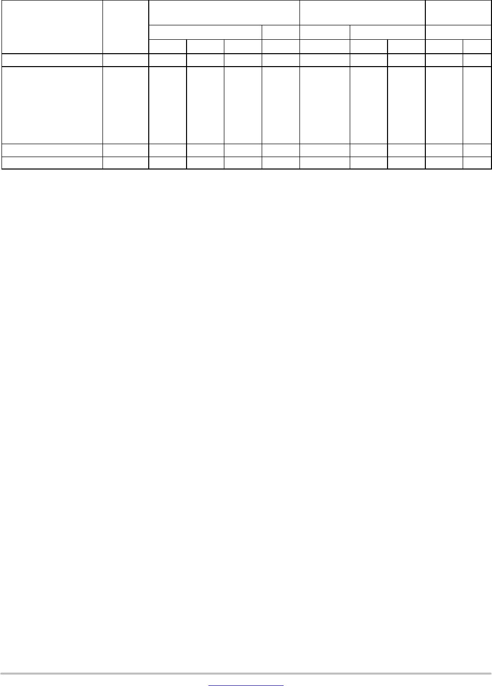
Device*
Device
Marking
Zener Voltage (Notes 6 and 7) Zener Impedance (Note 8)
Leakage Cur-
rent
V
Z
(Volts) @ I
ZT
Z
ZT
@ I
ZT
Z
ZK
@ I
ZK
I
R
@ V
R
Min Nom Max mA
W W
mA
mA
Volts
MMSZ5226CT1G TD 3.234 3.3 3.366 20 28 1600 0.25 25 1
MMSZ5231CT1G TG 4.998 5.1 5.202 20 17 1600 0.25 5 2
MMSZ5232CT1G TH 5.488 5.6 5.712 20 11 1600 0.25 5 3
MMSZ5245CT1G TK 14.70 15 15.30 8.5 16 600 0.25 0.1 11
MMSZ5248CT1G TL 17.64 18 18.36 7.0 21 600 0.25 0.1 14
MMSZ5250CT1G TN 19.60 20 20.40 6.2 25 600 0.25 0.1 15
MMSZ5252CT1G TQ 23.52 24 24.48 5.2 33 600 0.25 0.1 18
MMSZ5256CT1G TW 29.40 30 30.60 4.2 49 600 0.25 0.1 23
MMSZ5258CT1G TX 35.28 36 36.72 3.4 70 700 0.25 0.1 27
6. “C” Suffix Type numbers shown have a standard tolerance of ±2% on the nominal Zener voltages.
7. Nominal Zener voltage is measured with the device junction in thermal equilibrium at T
L
= 30°C ±1°C.
8. Z
ZT
and Z
ZK
are measured by dividing the AC voltage drop across the device by the ac current applied.
The specified limits are for I
Z(AC)
= 0.1 I
Z(dc)
with the AC frequency = 1 kHz.
*Includes SZ-prefix devices where applicable.