TDA7479 Electrical specification
5/12
2 Electrical specification
2.1 Thermal data
2.2 Absolute maximum ratings
2.3 Electrical characteristics
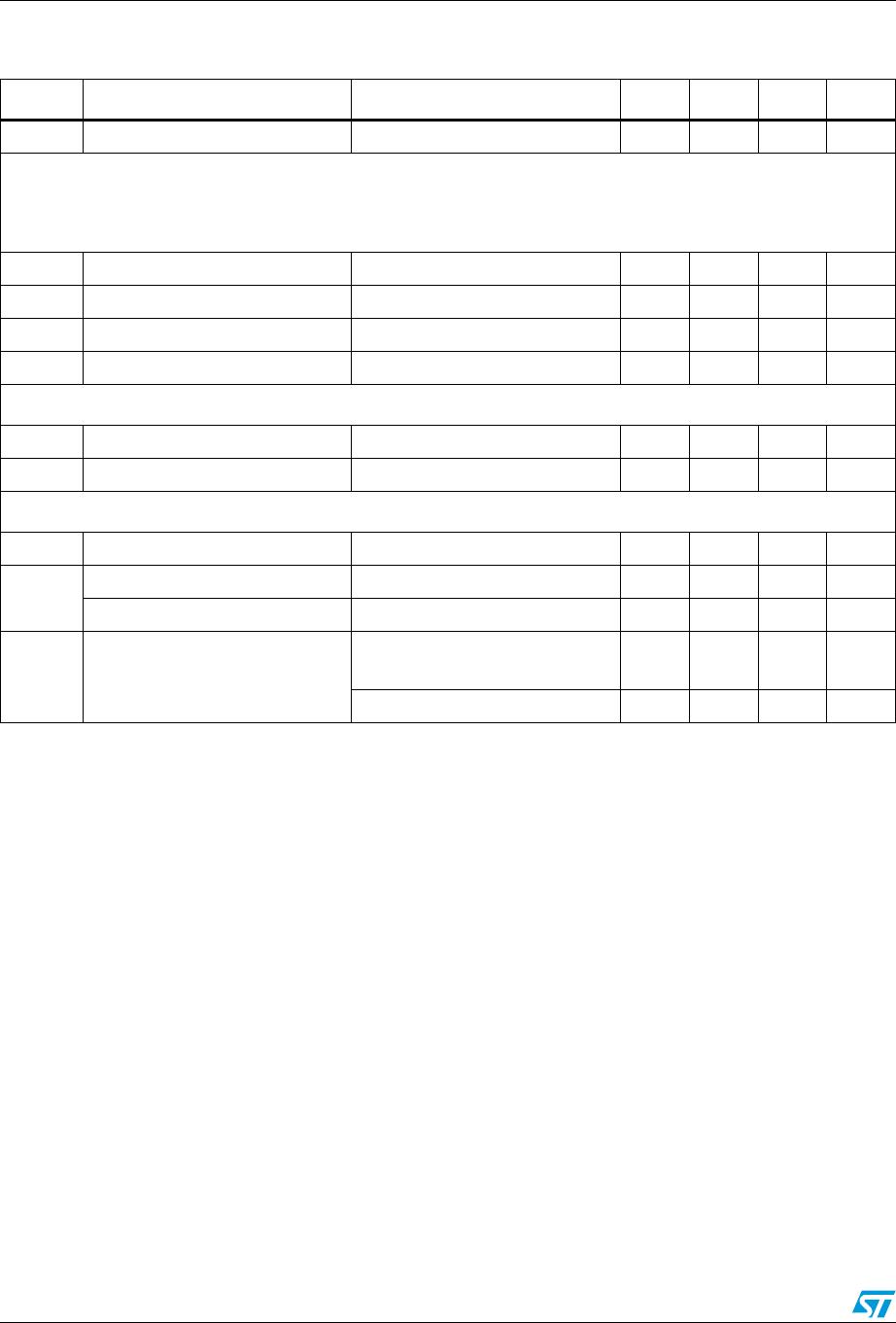
Table 3. Thermal data
Symbol Parameter SO16 TSSOP16 Unit
R
th j-case
Thermal resistance junction to case Max. 200 160 °C/W
Table 4. Absolute maximum ratings
Symbol Parameter Value Unit
V
S
Supply voltage -0.3 to 7 V
T
op
Operating temperature range -40 to 85 °C
T
stg
Storage temperature -55 to 150 °C
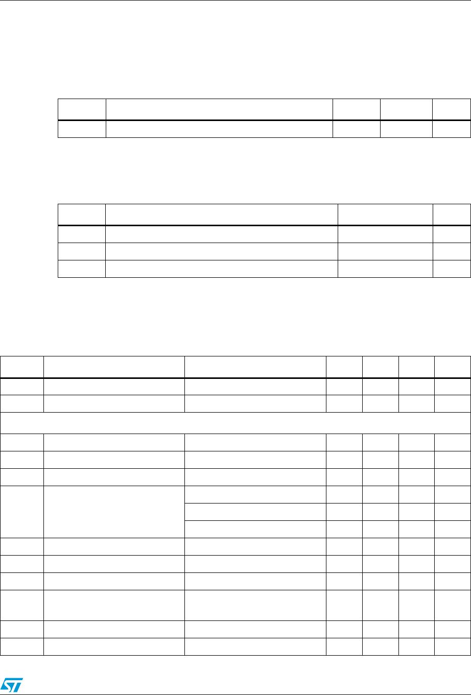
Table 5. Electrical characteristics
(T
amb
= 25°C, V
S
= 5V, unless otherwise specified)
Symbol Parameter Test condition Min. Typ. Max. Unit
V
S
Supply voltage 4.5 5 5.5 V
I
S
Supply current 7.5 11.0 mA
Filter
f
C
Center frequency 56.5 57 57.5 kHz
BW 3dB Bandwidth 2.5 3 3.5 kHz
G Gain f = 57 kHz 18 20 22 dB
A Attenuation
f ± 4 kHz 18 22 dB
f = 38 kHz 50 60 dB
f = 67 kHz 35 45 dB
R
I
Input impedance of MPX 80 120 150 K
R
L
Load impedance on FILOUT 1 M
S/N Signal to noise ratio V
IN
= 3 mVrms 30 40 dB
V
IN
MPX input signal
f = 19 kHz; T3 40 dB
(1)
f = 57 kHz (RDS+ ARI)
1000
50
mV
RMS
mV
RMS
S
RDS
RDS detection sensitivity 1 mVrms
S
ARI
ARI Detection Sensitivity 3 mVrms