LTC2631
16
2631fc
For more information www.linear.com/LTC2631
typical perFormance characteristics
LTC2631
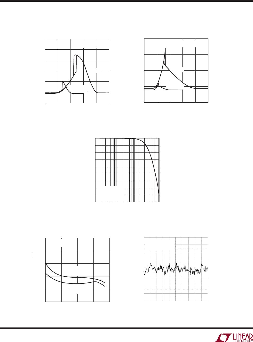
Multiplying Bandwidth
Noise Voltage vs Frequency
0.1Hz to 10Hz Voltage Noise
Supply Current vs Logic Voltage
Supply Current
vs REF_SEL Voltage
FREQUENCY (Hz)
100
NOISE VOLTAGE (nV/√Hz)
200
300
1M
2631 G34
100
0
1k
10k
100k
500
400
INTERNAL REF.
CODE = MIDSCALE
LTC2631-H
(V
CC
= 5V)
LTC2631-L
(V
CC
= 4V)
1s/DIV
10µV/DIV
2631 G35
LTC2631-L, V
CC
= 4V
INTERNAL REF.
CODE = MIDSCALE
LOGIC VOLTAGE (V)
0
I
CC
(mA)
1.2
0.8
0.4
1.0
0.6
0.2
0.0
42
2631 G31
531
V
CC
= 5V
V
CC
= 3V
(LTC2631-L)
SWEEP SCL AND SDA
BETWEEN 0V AND V
CC
REF_SEL VOLTAGE (V)
0
I
CC
(mA)
0.5
0.3
0.4
0.2
0.1
42
2631 G32
531
V
CC
= 5V
V
CC
= 3V
(LTC2631-L)
SWEEP REF_SEL
BETWEEN 0V AND V
CC
FREQUENCY (Hz)
1k
dB
0
–2
–6
–8
–14
–4
–12
–10
–16
–18
100k
2631 G33
1000k10k
V
CC
= 5V
V
REF(DC)
= 2V
V
REF(AC)
= 0.2V
P-P
CODE = FULL SCALE
T
A
= 25°C, unless otherwise noted.
LTC2631
17
2631fc
For more information www.linear.com/LTC2631
pin Functions
CA0 (Pin 1): Chip Address Bit 0. Tie this pin to V
CC
, GND
or leave it floating to select an I
2
C slave address for the
part (see Tables 1 and 2).
SCL (Pin 2): Serial Clock Input Pin. Data is shifted into the
SDA pin at the rising edges of the clock. This high impedance
pin requires a pull-up resistor or current source to V
CC
.
SDA (Pin 3): Serial Data Bidirectional Pin. Data is shifted
into the SDA pin and acknowledged by the SDA pin. This
pin is high impedance while data is shifted in. Open-drain
N-channel output during acknowledgment. SDA requires
a pull-up resistor or current source to V
CC
.
GND (Pin 4): Ground.
V
CC
(Pin 5): Supply Voltage Input. 2.7VV
CC
≤ 5.5V
(LTC2631-L) or 4.5VV
CC
≤ 5.5V (LTC2631-H). Bypass
to GND with a 0.1µF capacitor.
REF (Pin 6): Reference Voltage Input or Output. When
External Reference mode is selected, REF is an input (0V
V
REF
V
CC
) where the voltage supplied sets the full-
scale voltage. When Internal Reference is selected, the
10ppm/°C 1.25V (LTC2631-L) or 2.048V (LTC2631-H)
internal reference is available at the pin. This output may
be bypassed to GND with up to 10µF (0.33µF is recom-
mended), and must
be buffered when driving external DC
load current.
V
OUT
(Pin 7): DAC Analog Voltage Output.
CA1 (Pin 8, LTC2631-Z): Chip Address Bit 1. Tie this pin
to V
CC
, GND or leave it floating to select an I
2
C slave ad-
dress for the part (see Table 1).
REF_SEL (
Pin 8, LTC2631-M): Selects default Reference
at power up. Tie to V
CC
to select the Internal Reference,
or GND to select an External Reference. After power-up,
the logic state at this pin is ignored and the reference may
be changed only by software command.
LTC2631
18
2631fc
For more information www.linear.com/LTC2631
Block Diagrams
DAC
REGISTER
RESISTOR
DIVIDER
INTERNAL
REFERENCE
INPUT
REGISTER
I
2
C
INTERFACE
DAC
V
OUT
SWITCH
CONTROL
DECODE LOGIC
SDA
V
CC
REF
GND
DACREF
2631 BD
SCL
CA0
REF_SEL
I
2
C
ADDRESS
DECODE
DAC
REGISTER
RESISTOR
DIVIDER
INTERNAL
REFERENCE
INPUT
REGISTER
I
2
C
INTERFACE
DAC
V
OUT
SWITCH
CONTROL
DECODE LOGIC
SDA
V
CC
REF
GND
DACREF
SCL
CA1
CA0
I
2
C
ADDRESS
DECODE
test circuits
LTC2631-Z
LTC2631-M
100Ω
R
INH
/R
INL
/R
INF
V
IH(CAn)
/V
IL(CAn)
CAn
GND
2631 TC
V
CC
Test Circuit 2Test Circuit 1
CAn
Test Circuits for I
2
C Digital I/O (See Electrical Characteristics)

LTC2631AHTS8-HM12#TRPBF

Mfr. #:
Manufacturer:
Analog Devices Inc.
Description:
Digital to Analog Converters - DAC 12-Bit, 1LSB INL I2C DAC (4.096V ref, Reset to Mid-Scale)
Lifecycle:
New from this manufacturer.
Delivery:
DHL FedEx Ups TNT EMS
Payment:
T/T Paypal Visa MoneyGram Western Union