LTC5507ES6#TRMPBF

LTC5507
1
5507f
APPLICATIO S
U
DESCRIPTIO
U
FEATURES
TYPICAL APPLICATIO
U
Wireless Transceivers
Wireless and Cable Infrastructure
RF Power Alarm
Envelope Detector
Temperature Compensated Internal Schottky
Diode RF Detector
Wide Input Power Range: –34dBm to 14dBm
Ultra Wide Input Frequency Range: 100kHz to
1000MHz
Buffered Output
Wide V
CC
Range of 2.7V to 6V
Low Operating Current: 550µA
Low Shutdown Current: <2µA
Low Profile (1mm) ThinSOT
TM
Package
100kHz to 1GHz
RF Power Detector
The LTC
®
5507 is an RF power detector for applications
operating from 100kHz to 1000MHz. The input frequency
range is determined by an external capacitor. A tempera-
ture-compensated Schottky diode peak detector and buffer
amplifier are combined in a small 6-pin ThinSOT package.
The RF input voltage is peak detected using an on-chip
Schottky diode and external capacitor. The detected volt-
age is buffered and supplied to the V
OUT
pin. A power
saving shutdown mode reduces supply current to less
than 2µA.
, LTC and LT are registered trademarks of Linear Technology Corporation.
ThinSOT is a trademark of Linear Technology Corporation
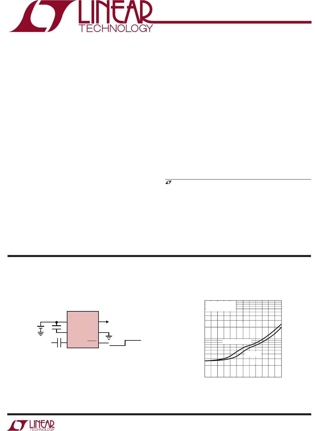
5507 TA01
V
OUT
GND
SHDN
V
CC
PCAP
RF
IN
LTC5507
4
5
6
3
2
1
V
OUT
DETECTED
VOLTAGE
V
BAT
2.7V TO 6V
C2
C1
RF
INPUT
DISABLE ENABLE
Figure 1. 100kHz to 1000MHz RF Power Detector
Typical Detector Characteristics
at 100kHz, 100MHz and 1000MHz
RF INPUT POWER (dBm)
V
OUT
OUTPUT VOLTAGE (mV)
10000
5507 TA01b
100
1000
–26 6 14–2–10–18
–34
100kHz, 100MHz
1000MHz
T
A
= 25°C
V
CC
= 2.7V TO 6V
LTC5507
2
5507f
V
CC
, V
OUT
to GND ....................................0.3V to 6.5V
RF
IN
Voltage to GND ......................... (V
CC
± 1.8V) to 7V
SHDN Voltage to GND ................ 0.3V to (V
CC
+ 0.3V)
PCAP Voltage to GND ........................(V
CC
– 1.8V) to 7V
I
VOUT
...................................................................... 5mA
Operating Temperature Range (Note 2) .. 40°C to 85°C
Maximum Junction Temperature ......................... 125°C
Storage Temperature Range ................ 65°C to 150°C
Lead Temperature (Soldering, 10 sec)................. 300°C
ORDER PART
NUMBER
S6 PART
MARKING
T
JMAX
= 125°C, θ
JA
= 250°C/W
LTZX
LTC5507ES6
ABSOLUTE AXI U RATI GS
W
WW
U
PACKAGE/ORDER I FOR ATIO
UUW
(Note 1)
ELECTRICAL CHARACTERISTICS
The denotes the specifications which apply over the full operating
temperature range, otherwise specifications are at T
A
= 25°C. V
CC
= 3.6V, RF Input Signal is Off, unless otherwise noted.
PARAMETER CONDITIONS MIN TYP MAX UNITS
V
CC
Operating Voltage 2.7 6 V
I
VCC
Shutdown Current SHDN = 0V 2 µA
I
VCC
Operating Current SHDN = V
CC
, I
VOUT
= 0mA 0.55 0.85 mA
V
OUT
V
OL
(No RF Input) R
LOAD
= 2k, SHDN = V
CC
, Enabled 130 250 370 mV
SHDN = 0V, Disabled 1 mV
V
OUT
Output Current V
OUT
= 1.75V, V
CC
= 2.7V to 6V, V
OUT
= 10mV 12 mA
V
OUT
Enable Time SHDN = V
CC
, C
LOAD
= 33pF, R
LOAD
= 2k 720 µs
V
OUT
Load Capacitance (Note 4) 33 pF
V
OUT
Noise V
CC
= 3V, Noise BW = 1.5MHz, 50 RF Input Termination 2 mV
P-P
SHDN Voltage, Chip Disabled V
CC
= 2.7V to 6V 0.35 V
SHDN Voltage, Chip Enabled V
CC
= 2.7V to 6V 1.4 V
SHDN Input Current SHDN = 3.6V 24 40 µA
RF
IN
Input Frequency Range 0.1– 1000 MHz
Max RF
IN
Input Power (Note 3) 14 dBm
RF
IN
AC Input Resistance F = 10MHz, RF Input = –10dBm 130
F = 1000MHz, RF Input = –10dBm 95
RF
IN
Input Shunt Capacitance 1.7 pF
Consult LTC Marketing for parts specified with wider operating temperature ranges.
Note 1: Absolute Maximum Ratings are those values beyond which the life
of a device may be impaired.
Note 2: Specifications over the –40°C to 85°C operating temperature
range are assured by design, characterization and correlation with
statistical process controls.
Note 3: RF performance is tested at: 80MHz, –4dBm
Note 4: Guaranteed by design.
6 RF
IN
5 PCAP
4 V
CC
SHDN 1
TOP VIEW
S6 PACKAGE
6-LEAD PLASTIC SOT-23
GND 2
V
OUT
3
LTC5507
3
5507f
TYPICAL PERFOR A CE CHARACTERISTICS
UW
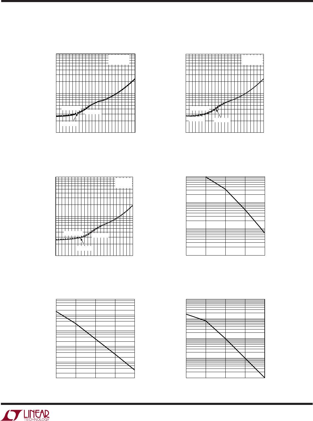
LTC5507 Typical Detector
Characteristics, 100kHz,
V
CC
= 2.7V TO 6V
Positive V
OUT
Slew Rate vs C2
Capacitance
LTC5507 Typical Detector
Characteristics, 1000MHz
V
CC
= 2.7V TO 6V
LTC5507 Typical Detector
Characteristics, 100MHz
V
CC
= 2.7V TO 6V
RF INPUT POWER (dBm)
–34 –28 –22 –16
V
OUT
OUTPUT VOLTAGE (mV)
100
1000
10000
–10 4 2 8 14
5507 G01
T
A
= –40°C
T
A
= 85°C
C1 = 0.47µF
C2 = 0.47µF
T
A
= 25°C
T
A
= –40°C
T
A
= 85°C
C1 = 1000pF
C2 = 1000pF
T
A
= 25°C
RF INPUT POWER (dBm)
–34 –28 –22 –16
V
OUT
OUTPUT VOLTAGE (mV)
100
1000
10000
–10 4 2 8 14
5507 G02
T
A
= –40°C
T
A
= 85°C
C1 = 33pF
C2 = 33pF
T
A
= 25°C
RF INPUT POWER (dBm)
–34 –28 –22 –16
V
OUT
OUTPUT VOLTAGE (mV)
100
1000
10000
–10 4 2 8 14
5507 G03
C2 CAPACITANCE (pF)
33
POSITIVE V
OUT
SLEW RATE (V/µs)
10.0
1.0
0.10
0.01
330 3300 33000033000
5507 G04
C2 CAPACITANCE (pF)
33 330 3300 33000033000
5507 G05
NEGATIVE V
OUT
SLEW RATE (V/µs)
10.000
1.000
0.100
0.010
0.001
0
C2 CAPACITANCE (pF)
33 330 3300 33000033000
5507 G06
V
OUT
BW (kHz)
10000
1000
100
10
1
V
OUT
BW vs C2 Capacitance
Negative V
OUT
Slew Rate vs C2
Capacitance

LTC5507ES6#TRMPBF

Mfr. #:
Manufacturer:
Analog Devices Inc.
Description:
RF Detector 100kHz to 1GHz RF Pwr Detector
Lifecycle:
New from this manufacturer.
Delivery:
DHL FedEx Ups TNT EMS
Payment:
T/T Paypal Visa MoneyGram Western Union

Products related to this Datasheet