LTC5507
5
5507f
APPLICATIO S I FOR ATIO
WUU
U
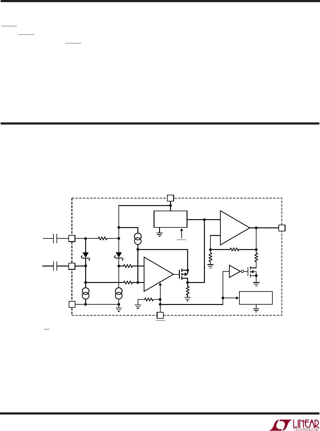
Operation
The LTC5507 integrates several functions to provide RF
power detection over frequencies up to 1000MHz. These
functions include an internally compensated buffer ampli-
fier, an RF Schottky diode peak detector and level shift
amplifier to convert the RF signal to DC, a delay circuit to
avoid voltage transients at V
OUT
when coming out of shut-
down, and a gain compression circuit to extend the
detector dynamic range.
Buffer Amplifier
The buffer amplifier has a gain of two and is capable of
driving a 2mA load. The buffer amplifier typically has an
output voltage range of 0.25V to V
CC
– 0.1V.
RF Detector
The internal RF Schottky diode peak detector and level
shift amplifier converts the RF input signal to a low
frequency signal. The frequency range of the RF pin is
typically up to 1000MHz. The detector demonstrates ex-
cellent operation over a wide range of input power. The
Schottky detector is biased at about 70µA. The hold
capacitor is external.
Gain Compression
The gain compression circuit changes the feedback ratio
as the RF peak-detected input voltage increases above
60mV. Below 60mV, the DC voltage gain from the peak
detector to the buffer output is 4. Above 140mV, the DC
voltage gain is reduced to 0.75. The compression expands
the low power detector range due to higher gain.
Modes of Operation
MODE SHDN OPERATION
Shutdown Low Disabled
Enable High Power Detect
Applications
The LTC5507 can be used as a self-standing signal strength
measuring receiver for a wide range of input signals from
–34dBm to 14dBm for frequencies up to 1000MHz.
The LTC5507 can be used as a demodulator for AM and
ASK modulated signals with data rates up to 1.5MHz.
Depending on specific application needs, the RSSI output
can be split into two branches, providing AC-coupled data
(or audio) output and DC-coupled, RSSI output for signal
strength measurements and AGC.
C1, C2 Capacitor Selection (Refer to Figure 3)
C1 couples the RF input signal to the detector input RF
IN
which is referenced to V
CC
. C2 is the peak detector
capacitor connected between PCAP and V
CC
. The value of
C2 will affect the slew rate and bandwidth. Typically C1 can
equal C2. Ceramic capacitors are recommended for C1
and C2. The values for C1 and C2 are dependent on the
operating RF frequency. The capacitive reactance should
be less than 5Ω to minimize ripple on C2.
C2(µF) ≥ 1/(30 • f) where f is the lowest RF input
frequency (MHz)
C1 = C2
In general, select C1 and C2 large enough to pass the
lowest expected RF signal frequency, as described by the
above formulas. But optimize C1 and C2, subject to this
constraint, to improve output slew rate and bandwidth,
and to enable good AC performance for the highest
expected RF signal frequency.