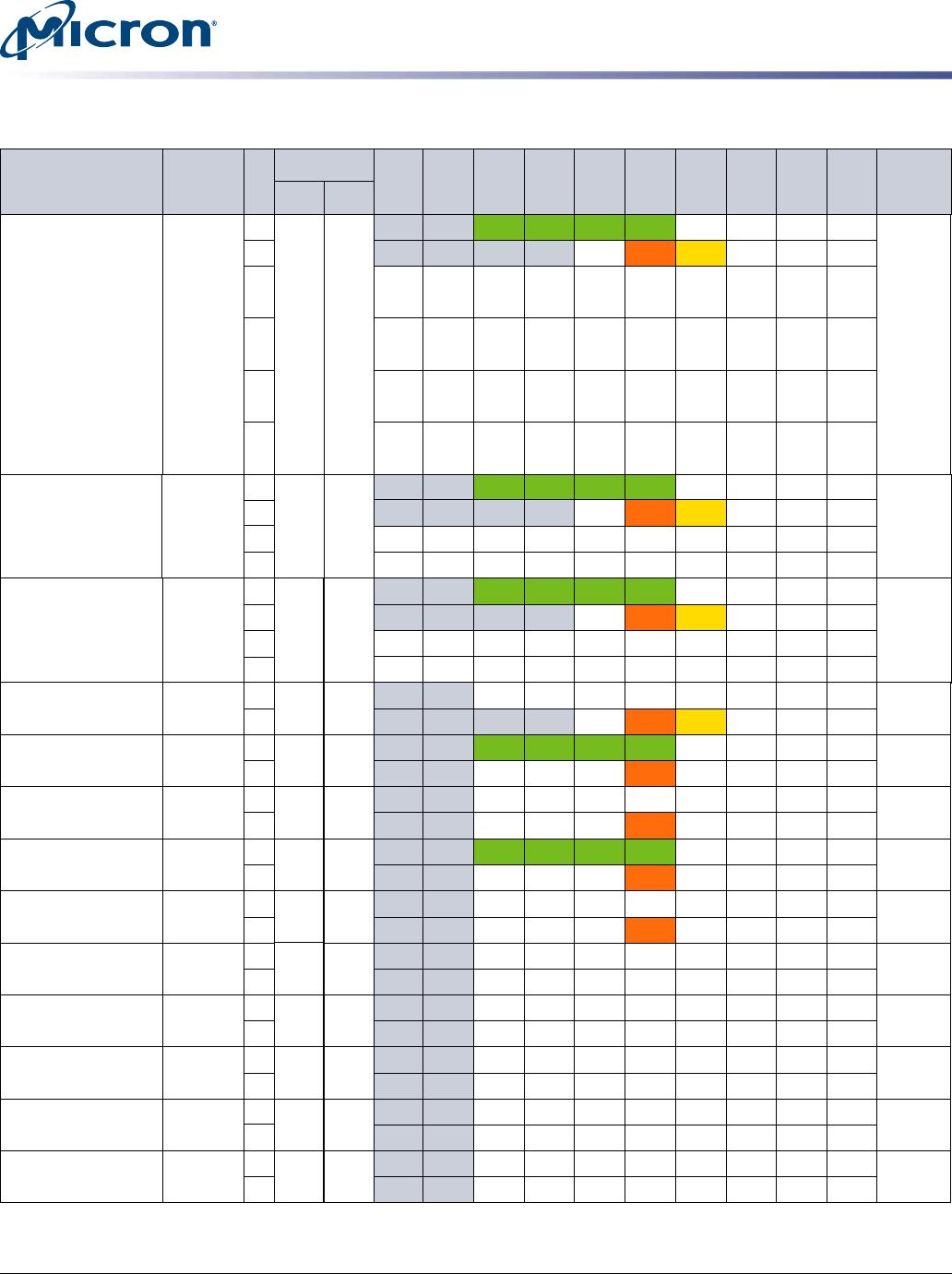
2. Values shown for CA[9:0] are logical values; the physical values are inverted when com-
mand/address bus inversion (CABI) is enabled and CABI_n = L.
3. M[3:0] provide the mode register address (MRA), OP[11:0] the opcode to be loaded.
4. BA[3:0] provide the bank address, R[13:0] provide the row address.
5. B[3:0] provide the bank address, C[6:0] provide the column address; no sub-word ad-
dressing within a burst of 16. BST[15:0] provide the write data mask for each burst posi-
tion with WDM(A) and WSM(A) commands.
6. CE (channel enable) is intended for PC mode. The command is active when CE = H.
When CE = L the data access is suppressed.
7. The command is REFRESH or PER-BANK REFRESH/PER-2-BANK REFRESH when CKE_n(n) =
L and SELF REFRESH ENTRY when CKE_n(n) = H.
8. B[3:0] select the burst position, and D[9:0] provide the data.
9. BA[3:0] provide the bank address.
10. All three encodings perform the same NOP. NOP (2) and NOP (3) encodings are only al-
lowed during CA Training.
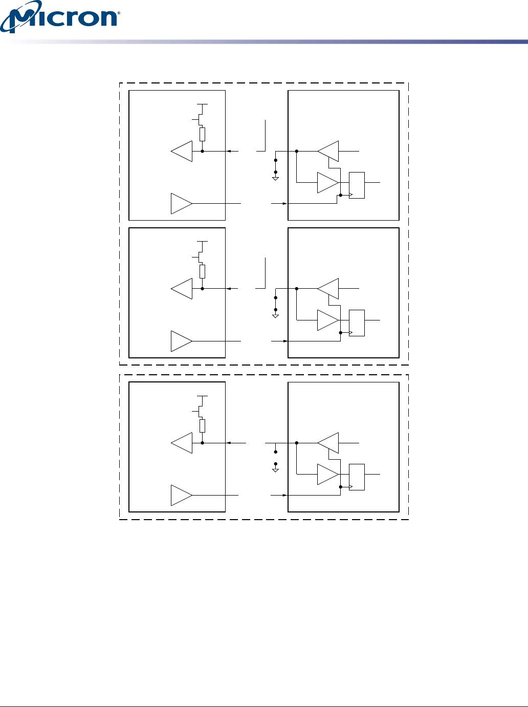
Clamshell (x8) Mode Enable
A GDDR6 SGRAM-based memory system is typically divided into several channels.
GDDR6 has been optimized for a 16-bit-wide channel. A channel can be comprised of a
single device operated in x16 mode, or two devices each operated in x8 mode. For x8
mode the devices are typically assembled on opposite sides of the PCB in what is refer-
red as a clamshell layout.
Whether in x16 mode or x8 mode the device will operate with a point-to-point connec-
tion on the high-speed data signals. The disabled signals in x8 mode should all be in a
High-Z state, non-terminating.
The x8 mode is detected at power-up on EDC1_A and EDC0_B. For x8 mode these sig-
nals are tied to V
SS
; they are part of the bytes that are disabled in this mode and there-
fore not needed for EDC functionality. For x16 mode these signals are active and always
terminated to V
DDQ
in the system or by the controller.
The configuration is set with RESET_n going HIGH. Once the configuration has been
set, it cannot be changed during normal operation. Typically, the configuration is fixed
in the system. Details of the x8 mode detection are depicted in Figure 8. A comparison
of x16 mode and x8 mode systems is shown in Figure 9.
Table 4: Clamshell (x8) Mode Enable
Mode EDC0_A EDC1_A EDC0_B EDC1_B
x8 V
DDQ
V
SS
(on board) V
SS
(on board) V
DDQ
x16 V
DDQ
(terminated by the system or controller)
8Gb: 2 Channels x16/x8 GDDR6 SGRAM
Functional Description
CCMTD-1412786195-10191
gddr6_sgram_8gb_brief.pdf - Rev. F 8/18 EN
11
Micron Technology, Inc. reserves the right to change products or specifications without notice.
© 2016 Micron Technology, Inc. All rights reserved.