LT3504
20
3504fa
For more information www.linear.com/LT3504
applicaTions inForMaTion
Bear in mind that significant power dissipation occurs in
Q1 during an overvoltage event. The MOSFET junction
temperature must be kept below its absolute maximum
rating. For the overvoltage transient shown in Figure 10,
MOSFET Q1 conducts 0.5A (full load on all buck channels)
while withstanding the voltage difference between V
SUPPLY
(180V peak) and V
IN
(33V). This results in a peak power of
74W. Since the overvoltage pulse in Figure 10 is roughly
triangular, average power dissipation during the transient
event (about 400ms) is approximately half the peak power.
As such, the average power is given by:
P
AVG
(W) =
•P
PEAK
(W) = 37W
In order to approximate the MOSFET junction temperature
rise from an overvoltage transient, one must determine
the MOSFET transient thermal response as well as the
MOSFET power dissipation. Fortunately, most MOSFET
transient thermal response curves are provided by the
manufacturer (as shown in Figure 11). For a 400ms pulse
duration, the FQB34N20L MOSFET thermal response
Z
ΘJC
(t) is 0.65°C/W. The MOSFET junction temperature
rise is given by:
°
=
=
°
Note that, by properly selecting MOSFET Q1, it is possible
to withstand even higher input voltage surges. Consult
manufacturer data sheets to ensure that the MOSFET
operates within its Maximum Safe Operating Area.
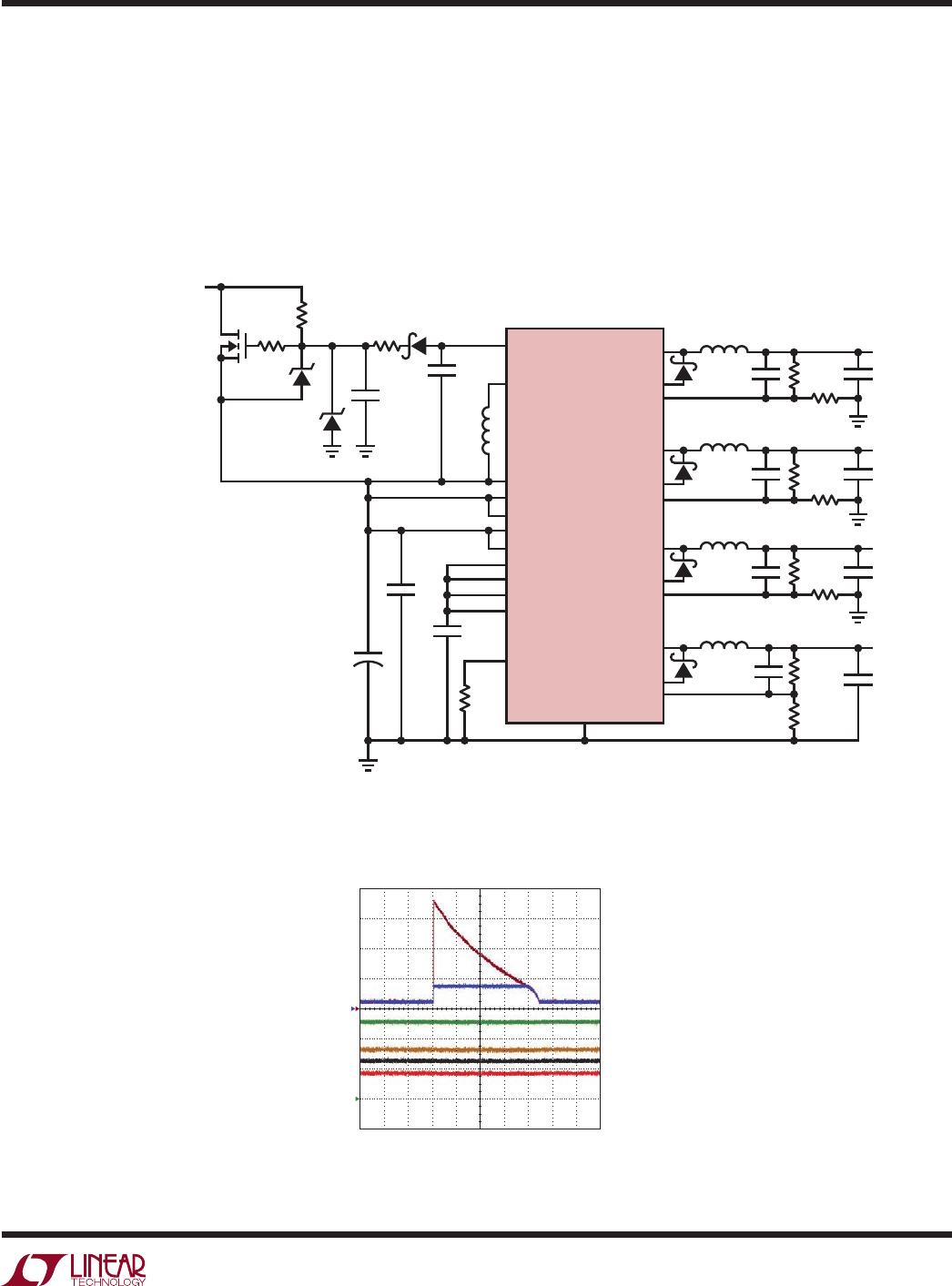
The application circuit start-up behavior is shown in
Figure 12. Resistor R2 pulls up on the gate of Q1, forcing
sour
ce-connected V
IN
to follow approximately 3V below
V
SUPPLY
. Once V
IN
reaches the LT3504’s 3.2V minimum
start-up voltage, the on-chip boost converter immedi-
ately regulates the V
SKY
rail 4.85V above V
IN
. Diode D3
and resistor R3 bootstrap Q1’s gate voltage to the V
SKY
,
fully enhancing Q1. This connects V
IN
directly to V
SUPPLY
through Q1’s low resistance drain-source path. It should
be noted that, prior to V
SKY
being present, the minimum
input voltage is about 6.2V. However, with V
SKY
in regulation
and Q1 enhanced, the minimum run voltage drops to 3.2V,
permitting the LT3504 to maintain regulation through deep
input voltage dips Figure 13 shows all channels operating
down to the LT3504’s 3.2V minimum input voltage.