3
COMMERCIAL AND INDUSTRIAL
TEMPERATURE RANGES
IDT72V01/72V02/72V03/72V04/72V05/72V06 3.3V ASYNCHRONOUS FIFO
512 x 9, 1,024 x 9, 2,048 x 9, 4,096 x 9, 8,192 x 9 and 16,384 x 9
AC ELECTRICAL CHARACTERISTICS
(1)
(Commercial: VCC = 3.3V ± 0.3V, TA = 0°C to +70°C; Industrial: VCC = 3.3V ± 0.3V, TA = –40°C to +85°C)
Commercial Com'l and Ind'l
(2)
Commercial
IDT72V01L15 IDT72V01L25 IDT72V01L35
IDT72V02L15 IDT72V02L25 IDT72V02L35
IDT72V03L15 IDT72V03L25 IDT72V03L35
IDT72V04L15 IDT72V04L25 IDT72V04L35
IDT72V05L15 IDT72V05L25 IDT72V05L35
IDT72V06L15 IDT72V06L25 IDT72V06L35
Symbol Parameter Min. Max. Min. Max. Min. Max. Unit
fS Shift Frequency — 40 — 28.5 — 22.2 M Hz
tRC Read Cycle Time 25 — 35 — 45 — ns
tA Access Time — 15 — 25 — 35 ns
tRR Read Recovery Time 10 — 10 — 10 — ns
tRPW Read Pulse Width
(3)
15 — 25 — 35 — ns
tRLZ Read Pulse Low to Data Bus at Low Z
(4)
3—3—3 —ns
tWLZ Write Pulse High to Data Bus at Low Z
(4,5)
5—5—5 —ns
tDV Data Valid from Read Pulse High 5 — 5 — 5 — ns
tRHZ Read Pulse High to Data Bus at High Z
(4)
— 15— 18— 20ns
tWC Write Cycle Time 25 — 35 — 45 — ns
tWPW Write Pulse Width
(3)
15 — 25 — 35 — ns
tWR Write Recovery Time 10 — 10 — 10 — ns
tDS Data Setup Time 11 — 15 — 18 — ns
tDH Data Hold Time 0 — 0 — 0 — ns
tRSC Reset Cycle Time 25 — 35 — 45 — ns
tRS Reset Pulse Width
(3)
15 — 25 — 35 — ns
tRSS Reset Setup Time
(4)
15 — 25 — 35 — ns
tRSR Reset Recovery Time 10 — 10 — 10 — ns
tRTC Retransmit Cycle Time 25 — 35 — 45 — ns
tRT Retransmit Pulse Width
(3)
15 — 25 — 35 — ns
tRTS Retransmit Setup Time
(4)
15 — 25 — 35 — ns
tRTR Retransmit Recovery Time 10 — 10 — 10 — ns
tEFL Reset to Empty Flag Low — 25 — 35 — 45 ns
tHFH,FFH Reset to Half-Full and Full Flag High — 25 — 35 — 45 ns
tRTF Retransmit Low to Flags Valid — 25 — 35 — 45 ns
tREF Read Low to Empty Flag Low — 15 — 25 — 30 ns
tRFF Read High to Full Flag High — 15 — 25 — 30 ns
tRPE Read Pulse Width after EF High 15 — 25 — 35 — ns
tWEF Write High to Empty Flag High — 15 — 25 — 30 ns
tWFF Write Low to Full Flag Low — 15 — 25 — 30 ns
tWHF Write Low to Half-Full Flag Low — 25 — 35 — 45 ns
tRHF Read High to Half-Full Flag High — 25 — 35 — 45 ns
tWPF Write Pulse Width after FF High 15 — 25 — 35 — ns
tXOL Read/Write to XO Low — 15— 25— 35ns
tXOH Read/Write to XO High — 15 — 25 — 35 ns
tXI XI Pulse Width
(3)
15 — 25 — 35 — ns
tXIR XI Recovery Time 10 — 10 — 10 — ns
t
XIS XI Setup Time 10 — 10 — 10 — ns
NOTES:
1. Timings referenced as in AC Test Conditions.
2. Industrial temperature range product for the 25ns speed grade is available as a standard device.
All other speed grades are available by special order.
3. Pulse widths less than minimum value are not allowed.
4. Values guaranteed by design, not currently tested.
5. Only applies to read data flow-through mode.
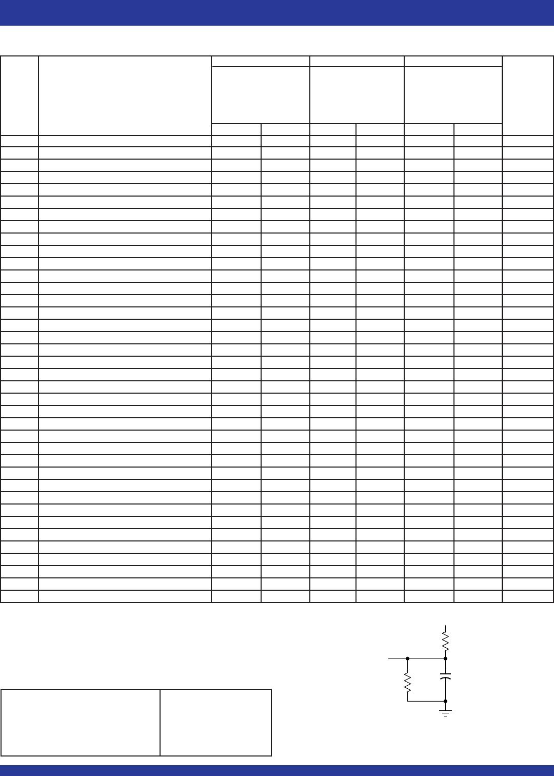
AC TEST CONDITIONS
Input Pulse Levels GND to 3.0V
Input Rise/Fall Times 5ns
Input Timing Reference Levels 1.5V
Output Reference Levels 1.5V
Output Load See Figure 1
Figure 1. Output Load
* Includes scope and jig capacitances.
or equivalent circuit
3033 drw 03
30pF*
330Ω
3.3V
D.U.T.
510Ω