3
IDT49FCT805BT/CT
FAST CMOS BUFFER/CLOCK DRIVER
MILITARY AND COMMERCIAL TEMPERATURE RANGES
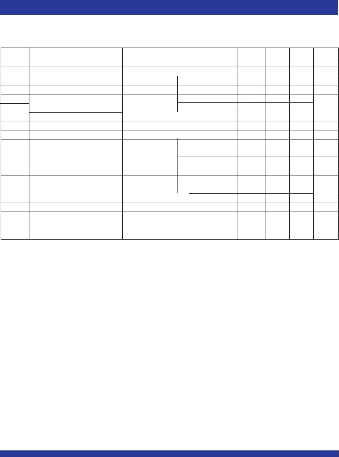
DC ELECTRICAL CHARACTERISTICS OVER OPERATING RANGE
Following Conditions Apply Unless Otherwise Specified:
Commercial: TA = 0°C to +70°C, Military: TA = -55°C to +125°C, VCC = 5V ± 10%
Symbol Parameter Test Conditions
(1)
Min. Typ.
(2)
Max. Unit
VIH Input HIGH Level Guaranteed Logic HIGH Level 2 — — V
VIL Input LOW Level Guaranteed Logic LOW Level — — 0.8 V
IIH Input HIGH Current
(5)
VCC = Max. VI = 2.7V — — ±1µA
IIL Input LOW Current
(5)
VCC = Max. VI = 0.5V — — ±1µA
I
OZH High Impedance Output Current VCC = Max. VO = 2.7V — — ±1µA
IOZL (3-State Output Pins) VO = 0.5V — — ±1
II Input HIGH Current VCC = Max., VI = VCC (Max.) — — ±1µA
VIK Clamp Diode Voltage VCC = Min., IIN = –18mA — –0.7 –1.2 V
IOS Short Circuit Current VCC = Max., VO = GND
(3)
–60 –120 –255 mA
V
CC = Min. IOH = –12mA MIL 2.4 3.3 — V
V
OH Output HIGH Voltage VIN = VIH or VIL IOH = –15mA COM'L
IOH = –24mA MIL 2 3 — V
IOH = –32mA COM'L
(4)
VOL Output LOW Voltage VCC = Min. IOL = 32mA MIL — 0.3 0.55 V
VIN = VIH or VIL IOL = 48mA COM'L
IOFF Input/Output Power Off Leakage
(5)
VCC = 0V, VIN or VO ≤ 4.5V — — ±1µA
VH Input Hysteresis for all inputs — — 150 — mV
ICCL Quiescent Power Supply Current VCC = Max., VIN = GND or VCC — 5 500 µA
ICCH
ICCZ
NOTES:
1. For conditions shown as Max. or Min., use appropriate value specified under Electrical Characteristics for the applicable device type.
2. Typical values are at Vcc = 5V, +25°C ambient.
3. Not more than one output should be shorted at one time. Duration of the test should not exceed one second.
4. Duration of the condition should not exceed one second.
5. The test limit for this parameter is ±5µA at TA = -55°C.